


VLSI Design Articles
Why Chips Fail: A Basic Guide to Chip Defects and IC Failure Analysis
Fun Facts About the Semiconductor Industry
Why Are Semiconductor Chips Expensive? Manufacturing Cost Explained
Instruction Set Architecture: How ISA Shapes Modern Chip Design


Get In Touch For Details! Request More Information
What is Physical Design in VLSI? A Comprehensive Guide to the Chip Layout Process
Aug 03, 2026 5 Min Read 296 Views
(Last Updated)
Table of contents
- TL;DR Summary
- Introduction
- Understanding Physical Design in VLSI
- What is Physical Design?
- Key Objectives of Physical Design
- Difference Between Frontend and Backend VLSI
- The Physical Design Flow
- Floorplanning
- Placement
- Clock Tree Synthesis
- Routing
- Physical Verification
- Key Tools in Physical Design
- Cadence Digital IC Design Platform
- Synopsys Galaxy Design Platform
- Mentor Graphics (Siemens EDA)
- Challenges in VLSI Physical Design
- Sub-Micron Effects
- Power Management Complexity
- Advanced Packaging Requirements
- Career Opportunities in Backend VLSI
- Job Roles
- Major employers include:
- Did You Know?
- Real-World Applications of Physical Design in VLSI
- Smartphone Processors
- Data Center Chips
- Automotive Semiconductors
- Common Mistakes in Physical Design in VLSI
- Ignoring Power Planning Early
- Overlooking Congestion Analysis
- Insufficient Timing Budgeting
- Neglecting Physical Verification Throughout
- Underestimating Iteration Requirements
- Why Learn Physical Design in VLSI at HCL GUVI?
- Conclusion
- Frequently Asked Questions
- What skills are required for physical design engineering?
- How long does it take to learn physical design?
- Is physical design a good career choice?
- What is the difference between place and route and physical design?
- Which companies hire physical design engineers?
- What tools are commonly used in physical design?
TL;DR Summary
- Physical Design in VLSI is the process of transforming a circuit design from logical representation to physical layout ready for fabrication.
- The PD flow includes floorplanning, placement, routing, and verification stages.
- Key tools include Cadence Innovus and Synopsys IC Compiler.
- Physical design engineers are in high demand in semiconductor companies like Intel, AMD, and NVIDIA.
- Our VLSI Design Course prepares professionals for careers in this field with hands-on projects and industry mentorship.
Introduction
In today’s digital world, integrated circuits power everything from smartphones to supercomputers. But how do these tiny chips transform from abstract designs to physical reality? The answer lies in Physical Design in VLSI (Very Large Scale Integration).
As Moore’s Law continues to drive chip complexity, the role of physical design has become increasingly critical. Modern processors contain billions of transistors that must be precisely arranged and connected while meeting stringent performance, power, and area constraints.
If you’re considering a career in semiconductor design, understanding physical design is essential. This guide breaks down the complex world of VLSI physical design into digestible concepts, showing you exactly what happens when circuits move from schematic to silicon.
Understanding Physical Design in VLSI
What is Physical Design?
Physical Design in VLSI refers to the process of converting a logical circuit design into a physical representation that can be fabricated on a silicon wafer.
While front-end design focuses on functionality and logic, physical design deals with the actual layout of components on a chip.
Think of physical design as architecture for microchips. Just as architects convert blueprints into livable buildings, physical design engineers translate circuit schematics into manufacturable layouts.
This involves placing millions of transistors, defining metal interconnections, and ensuring the final product meets performance specifications.
Want to understand where physical design fits in the semiconductor ecosystem? Read our guide on Semiconductor Value Chain: From Design to Delivery to see how chip design, fabrication, testing, and packaging come together.
Key Objectives of Physical Design
Physical design aims to achieve several critical goals:
- Area Minimization: Efficiently utilize silicon real estate
- Performance Optimization: Meet timing constraints and speed targets
- Power Efficiency: Reduce energy consumption while maintaining functionality
- Manufacturability: Ensure the design can be successfully fabricated
- Reliability: Create robust circuits that operate under various conditions
India’s semiconductor industry is creating exciting opportunities for backend VLSI engineers. Discover how the India Semiconductor Mission is driving demand for chip design professionals and shaping the future of semiconductor careers.
Difference Between Frontend and Backend VLSI
| Aspect | Frontend VLSI | Backend VLSI |
| Focus | Functional specification | Physical realization |
| Output | RTL code | GDSII layout file |
| Tools | HDL simulators | Place and route tools |
| Concerns | Logic correctness | Timing, power, area |
The Physical Design Flow
| Stage | Purpose |
| Floorplanning | Organize chip blocks |
| Placement | Position standard cells |
| Clock Tree Synthesis | Build clock network |
| Routing | Connect components |
| Verification | Validate manufacturability |
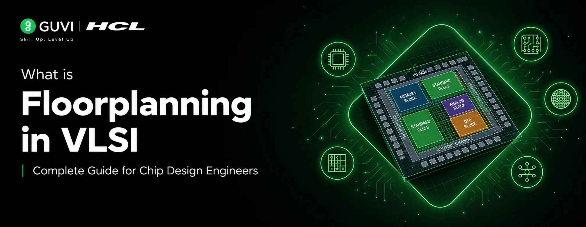
Floorplanning
Floorplanning is the initial stage where the chip’s overall organization is established. During this phase, designers determine the positions of major functional blocks, define power distribution networks, and allocate space for interconnect routing.
Key activities in floorplanning include:
- Defining core area and die dimensions
- Placing I/O pads around chip perimeter
- Allocating space for power and ground rings
- Positioning hard macros (RAMs, ROMs, analog blocks)
- Creating initial wire planning estimates
Modern floorplanning tools use sophisticated algorithms to optimize block placement based on connectivity patterns, helping minimize wire lengths and reduce signal delays.
Placement
After floorplanning, the placement stage positions all standard cells within the defined areas. Standard cells include basic logic gates like AND, OR, NAND, NOR, flip–flops, and buffers.
There are two main types of placement:
- Global Placement: Initial rough positioning of cells
- Detailed Placement: Fine-tuning cell positions to meet design rules
Placement algorithms consider factors like:
- Timing constraints
- Power density distribution
- Congestion avoidance
- Thermal considerations
During placement, place and route tools continuously evaluate timing paths and adjust cell positions accordingly to meet performance targets.
Clock Tree Synthesis
Clock distribution is one of the most challenging aspects of physical design. Clock Tree Synthesis (CTS) creates a balanced network to distribute clock signals to all sequential elements simultaneously.
Key CTS objectives include:
- Minimizing clock skew (timing difference between receivers)
- Reducing latency (signal propagation delay)
- Balancing power consumption across the clock network
- Ensuring signal integrity
Advanced CTS techniques use programmable clock buffers and mesh structures to achieve optimal clock distribution in high-performance designs.
Routing
Routing establishes electrical connections between components according to the netlist. This multi-layer process involves:
- Global routing (defining approximate paths)
- Detailed routing (precise track assignments)
- Via insertion (vertical connections between layers)
Modern chips use 10-15 metal layers for routing, with each layer having specific characteristics:
- Lower layers: Short local connections
- Middle layers: Medium-range routing
- Upper layers: Long global connections
Routing congestion management is crucial to avoiding “hotspots” where too many wires compete for limited routing resources.
Artificial Intelligence is changing backend chip design. Learn how AI-powered EDA tools are improving placement, routing, timing optimization, and verification in our guide on AI is Transforming the Semiconductor Industry.
Physical Verification
Before tape-out (final manufacturing data release), extensive physical verification ensures the design meets all requirements. This includes:
- Design Rule Checking (DRC): Validates layout against foundry manufacturing constraints
- Layout vs. Schematic (LVS): Ensures layout matches intended circuit functionality
- Electrical Rule Checking (ERC): Identifies potential electrical issues
- Antenna Checks: Prevents charge accumulation during manufacturing
Any violations discovered during verification require iterations between physical design and verification teams until all checks pass.
Key Tools in Physical Design
Industry-standard tools dominate the physical design landscape:
Cadence Digital IC Design Platform
- Innovus Implementation System (primary place and route tool)
- Encounter Conformal LEC (logic equivalence checking)
- Tempus Timing Signoff
Synopsys Galaxy Design Platform
- IC Compiler II (place and route)
- Design Compiler Graphical (synthesis)
- PrimeTime (static timing analysis)
Mentor Graphics (Siemens EDA)
- Calibre platform for physical verification
- Nitro-AMS for analog/mixed-signal design
These tools cost hundreds of thousands of dollars annually, making university-level access rare.
Challenges in VLSI Physical Design
Today’s chip designs present numerous challenges:

Sub-Micron Effects
As feature sizes shrink below 10nm, quantum effects become significant:
- Increased leakage power
- Variability in device characteristics
- Electromigration concerns
Power Management Complexity
Modern SoCs integrate multiple voltage domains requiring:
- Level shifters between domains
- Power gating mechanisms
- Dynamic voltage scaling
Advanced Packaging Requirements
2.5D and 3D integration techniques add new physical design dimensions:
- Through-silicon vias (TSVs)
- Interposer routing
- Thermal management
Career Opportunities in Backend VLSI
Backend VLSI design offers excellent career prospects with competitive salaries.
According to industry reports, entry-level physical design engineers earn 5−7 LPA annually in Silicon Valley, with experienced professionals commanding 20−25 LPA.
Job Roles
- Physical Design Engineer
- CAD Engineer
- DFT (Design for Test) Engineer
- Sign-off Engineer
- P&R Methodology Engineer
Major employers include:
- Intel
- AMD
- NVIDIA
- Qualcomm
- Broadcom
- Marvell
- MediaTek
Did You Know?
The Apple M1 chip contains over 16 billion transistors packed into just 120mm². To put this in perspective, if each transistor were the size of a marble, the entire chip would cover an area larger than 30 football fields!
Physical design engineers made this incredible feat possible through careful optimization of placement, routing, and power distribution.
The Apple M1 chip contains over 16 billion transistors packed into just 120mm². To put this in perspective, if each transistor were the size of a marble, the entire chip would cover an area larger than 30 football fields! Physical design engineers made this incredible feat possible through careful optimization of placement, routing, and power distribution.
Real-World Applications of Physical Design in VLSI
Smartphone Processors
Apple’s A-series chips exemplify modern physical design excellence. The A15 Bionic processor uses 5nm technology with advanced power management techniques implemented during physical design phases.
Data Center Chips
AMD’s EPYC processors demonstrate large-scale physical design challenges with chiplets containing billions of transistors connected through Infinity Fabric interconnects designed during physical implementation.
Automotive Semiconductors
NVIDIA’s DRIVE, Atlan platform for autonomous vehicles requires specialized physical design approaches to handle extreme temperature ranges (-40°C to 125°C) while maintaining automotive safety standards.
Common Mistakes in Physical Design in VLSI
1. Ignoring Power Planning Early
Many beginners focus solely on timing closure without considering power distribution networks, leading to IR drop violations that require costly redesigns.
2. Overlooking Congestion Analysis
Jumping straight into detailed placement without analyzing routing congestion often results in unrouteable designs that require significant restructuring.
3. Insufficient Timing Budgeting
Failing to properly allocate timing budgets across different design stages can result in last-minute timing violations that are expensive to fix.
4. Neglecting Physical Verification Throughout
Waiting until final sign-off to run DRC/LVS checks can reveal fundamental issues requiring architectural changes rather than localized fixes.
5. Underestimating Iteration Requirements
Physical design rarely progresses linearly. Expect 10-20 iterations between implementation and final sign-off, especially for first-time designs.
Why Learn Physical Design in VLSI at HCL GUVI?
HCL GUVI’s VLSI Design Course provides comprehensive training in physical design with:
- Hands-on labs using industry-standard tools
- Real-world projects mirroring actual industry workflows
- Mentorship from practicing physical design engineers
- Placement assistance with top semiconductor companies
- Flexible learning schedule for working professionals
Unlike traditional academic programs that focus on theory, our curriculum emphasizes practical skills demanded by today’s semiconductor industry.
Students work on actual chip layouts, experiencing the same challenges faced by professionals in companies like Intel and AMD.
Conclusion
Physical Design in VLSI represents the bridge between conceptual circuit ideas and tangible silicon products.
As chips become more complex with each technology node, skilled physical design engineers remain in high demand across the semiconductor industry.
Understanding the intricate processes involved in VLSI physical design from floorplanning to physical verification provides insight into one of technology’s most critical disciplines.
Through proper education and hands-on experience, you can contribute to creating the next generation of electronic devices that will shape our technological future.
Frequently Asked Questions
1. What skills are required for physical design engineering?
Essential skills include digital design fundamentals, scripting languages (Tcl, Perl, Python), understanding of CMOS technology, and familiarity with EDA tools like Cadence or Synopsys platforms.
2. How long does it take to learn physical design?
With dedicated study, foundational concepts can be grasped in 3-6 months. However, becoming proficient requires 1-2 years of hands-on experience working on real projects.
3. Is physical design a good career choice?
Yes, physical design offers excellent career prospects with strong job security and competitive compensation. The global semiconductor shortage has further increased demand for skilled physical design engineers.
4. What is the difference between place and route and physical design?
Place and route refers specifically to the placement and routing stages within the broader physical design flow. Physical design encompasses all implementation activities from floorplanning to final sign-off.
5. Which companies hire physical design engineers?
Leading semiconductor companies including Intel, AMD, NVIDIA, Qualcomm, Broadcom, and Marvell actively recruit physical design engineers. Fabless companies like Apple and Google also maintain substantial physical design teams.
6. What tools are commonly used in physical design?
Industry-standard tools include Cadence Innovus, Synopsys IC Compiler, and Mentor Graphics Calibre. Most professionals gain exposure to these through specialized training programs.
Success Stories

About the Author
Hashmithaa
Hi, I’m Hashmithaa — a content writer with a love for words. Writing isn’t just what I do; it’s how I connect, communicate, and create meaning in a noisy digital world. And if my words help someone make a better decision, learn something new, or feel more confident, then I’ve done my job well.
View all posts by Hashmithaa
Connect with me @














Did you enjoy this article?