


VLSI Design Articles
Why Chips Fail: A Basic Guide to Chip Defects and IC Failure Analysis
Fun Facts About the Semiconductor Industry
Why Are Semiconductor Chips Expensive? Manufacturing Cost Explained
Instruction Set Architecture: How ISA Shapes Modern Chip Design


Get In Touch For Details! Request More Information

Top 8 VLSI Design Challenges in 2026: Solutions for Students & Engineers
Sep 10, 2026 8 Min Read 10845 Views
(Last Updated)
Table of contents
- TL;DR
- What do VLSI Designers Do?
- Top 8 VLSI Design Challenges in 2026
- VLSI Design Challenges Comparison Table
- 1) Increasing Design Complexity
- Ways to Overcome:
- 2) Power Management Issues
- Ways to Overcome:
- 3) Signal Integrity and Timing Closure
- Ways to Overcome:
- 4) Debugging and Verification Challenges
- Ways to Overcome:
- 5) Electromagnetic Interference (EMI) and Electromagnetic Compatibility (EMC) Issues
- Ways to Overcome:
- 6) Manufacturability and Yield Optimization
- Ways to Overcome:
- 7) Cost and Time-to-Market Pressures
- Ways to Overcome:
- 8) Interdisciplinary Skills Requirement
- Ways to Overcome:
- Best VLSI Design Practices and Challenges in India 2026
- How AI and Modern EDA Tools Are Changing VLSI Design in 2026
- Takeaways…
- FAQs
- What are the main VLSI design challenges in 2026?
- Why is VLSI design becoming more difficult?
- How can VLSI designers overcome power management challenges?
- Why is verification a major challenge in VLSI design?
- What skills are required to become a VLSI designer in 2026?
TL;DR
- The 8 biggest VLSI design challenges in 2026 are design complexity, power and thermal management, timing closure, verification, EMI/EMC, manufacturing yield, cost and time-to-market, and interdisciplinary skills.
- Modern VLSI teams are increasingly using AI-assisted EDA, advanced verification, hierarchical design, multiphysics analysis, power optimization, and design-for-manufacturing techniques to handle these challenges.
VLSI design challenges in 2026 are more complex than at any point in semiconductor history, verification bottlenecks alone consume over 70% of the typical design cycle.
As chips shrink to 3nm and below, designers face compounding problems: more transistors, more heat, more noise, tighter margins, and shorter time-to-market windows.
This guide breaks down the eight most critical VLSI design challenges engineers face today, explains why each one is getting harder, and gives you concrete, proven solutions to overcome them.
What do VLSI Designers Do?
VLSI designers are the brains behind microchips and integrated circuits that power everything from smartphones to autonomous vehicles.
These professionals have the complex job of fitting thousands, sometimes millions, of transistors onto a single chip. They carefully engineer integrated circuits through several key stages.
The process starts when they understand what’s needed and turn those needs into logical blueprints.

VLSI designers use specialized Computer-Aided Design (CAD) tools to place and connect millions of transistors, capacitors, and resistors on silicon substrates.
They focus on making three things better: speed, power consumption, and area utilization.
VLSI designers combine their knowledge of digital and analog circuitry with expertise in specialized tools and methods.
Their work helps advance semiconductor technology and makes them essential in today’s fast-changing world of electronic innovation.
Want to understand the VLSI career path better? Explore our guide on How to Become a VLSI Designer in 2026 to learn about the skills, qualifications, specializations, and career path you can follow.
Chiplets can let multiple smaller dies work together like one powerful chip. This approach is becoming increasingly important for high-performance AI and computing systems in 2026.
Top 8 VLSI Design Challenges in 2026
The semiconductor industry is entering a period of rapid growth driven by AI, high-performance computing, advanced communications, automotive electronics, and other applications.
Global semiconductor sales reached $795.6 billion in 2025, while WSTS projected worldwide semiconductor sales of $1.5 trillion for 2026.
This growth is also increasing the complexity of the chips engineers need to design.
VLSI Design Challenges Comparison Table
| VLSI Design Challenge | Why It Is Difficult in 2026 | Major Impact | Common Solutions |
| Design complexity | Advanced nodes, large SoCs, and multi-die architectures increase design interactions | Longer development and closure cycles | Hierarchical design, IP reuse, AI-assisted EDA |
| Power and thermal management | Higher transistor density increases power and thermal constraints | Battery life, performance and reliability | Power gating, DVFS, thermal-aware design |
| Signal integrity & timing | Dense interconnects and tighter timing margins increase closure difficulty | Performance and reliability | STA, crosstalk analysis, clock optimization |
| Verification & debugging | Complex SoCs create enormous verification and debug workloads | Delayed tapeout and higher engineering effort | Formal verification, emulation, AI-assisted debug |
| EMI/EMC | Higher switching activity and system complexity increase electromagnetic effects | Reliability and compliance | Shielding, grounding, simulation and pre-compliance testing |
| Manufacturability & yield | Advanced processes are more sensitive to variation and defects | Lower yield and higher costs | DFM, process modeling, yield analysis |
| Cost & time-to-market | Advanced chip development requires expensive design and manufacturing resources | Higher project risk | Automation, reusable IP, cloud/HPC resources |
| Interdisciplinary skills | Chip development increasingly connects hardware, software, and system engineering | Skill gaps and slower collaboration | Continuous learning and cross-domain training |
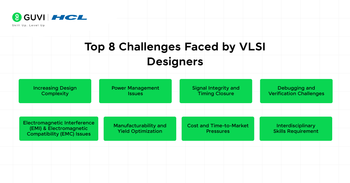
Let’s discuss these challenges and some ways to overcome or avoid them:
1) Increasing Design Complexity
One of the biggest VLSI design challenges in 2026 is the growing complexity of modern chips.
Advanced SoCs integrate billions of transistors across logic, memory, high-speed interfaces, AI accelerators, security engines, and third-party IP blocks.
As designs move toward advanced process technologies such as 3nm and below, along with chiplet- and multi-die architectures, engineers must manage increasingly complex interactions while meeting strict power, performance, area, reliability, and manufacturability targets.
This complexity extends beyond the number of components on a chip. Designers must integrate IP blocks from different sources, coordinate multiple clock and power domains, and ensure reliable communication across increasingly dense interconnects.
Advanced nodes also introduce tighter design rules, greater process variation, routing congestion, smaller timing and power margins, and more difficult power-delivery and thermal constraints.
As a result, placement, routing, verification, and design closure have become system-level optimization problems rather than isolated implementation tasks.
Ways to Overcome:
- Hierarchical Design Approach: Implement modular and hierarchical design techniques to manage complexity efficiently.
- AI & ML in Design Automation: Use AI-driven Electronic Design Automation (EDA) tools for optimized layout, verification, and debugging.
- Design Reuse & IP Integration: Utilize pre-verified intellectual property (IP) blocks to reduce development time and design risks.
- Advanced Verification Techniques: Employ formal verification, hardware emulation, and digital twins to validate designs early.
- Collaborative Design Workflows: Leverage cloud-based design platforms to enhance collaboration and parallel development.
Modern EDA platforms are moving beyond conventional automation. For example, Synopsys introduced newer AI-assisted and autonomous workflows in 2026, while Cadence expanded AI-driven capabilities across implementation and system analysis.
2) Power Management Issues
Power management remains a major challenge because modern chips must deliver higher performance without exceeding strict energy and thermal limits.
This challenge affects mobile devices, data centers, AI accelerators, and high-performance computing systems.
Power consumption generally comes from dynamic switching activity and leakage. Dynamic power is consumed when transistors switch between logic states, while short-circuit power is wasted when PMOS and NMOS transistors conduct simultaneously during transitions.
Leakage power is consumed even when transistors are idle, and advanced process nodes can increase leakage because of lower threshold voltages, tighter voltage margins, and greater process variation.
Designers must also consider power integrity, voltage variations, IR drop, electromigration, and thermal hotspots.
For mobile devices, excessive power reduces battery life and increases heat generation. For AI and high-performance computing systems, high power consumption increases cooling requirements, operating costs, and reliability risks.
As computing workloads continue to grow, power optimization has become essential not only for extending battery life but also for controlling the energy and infrastructure costs of large-scale systems.
Ways to Overcome:
- Low-Power Design Techniques: Implement clock gating, power gating, and dynamic voltage and frequency scaling (DVFS) to minimize power usage.
- Advanced Transistor Technologies: Use FinFETs, Gate-All-Around (GAA) FETs, and other low-leakage transistor architectures to reduce power leakage.
- Efficient Power Delivery Networks (PDNs): Optimize PDN design with decoupling capacitors and advanced power grid architectures to improve power integrity.
- AI-Driven Power Optimization: Leverage AI/ML algorithms for dynamic power management and predictive analysis in chip design.
- Thermal-Aware Design: Integrate advanced cooling solutions, such as 3D stacking with efficient heat dissipation techniques, to manage power-related thermal challenges.
In 2026, EDA vendors are increasingly integrating these analyses. Synopsys, for example, introduced Multiphysics Fusion solutions that combine timing, power integrity, thermal and electromagnetic analysis for advanced designs.
3) Signal Integrity and Timing Closure
As transistor dimensions and interconnect geometries shrink, signal integrity and timing closure become increasingly difficult.
Advanced-node designs also face greater variation in interconnect resistance, capacitance, power delivery, and temperature, making predictable timing and noise behavior more challenging.
Closely spaced wires can create crosstalk, coupling noise, and signal-integrity problems, particularly in dense routing regions and high-speed interfaces.
Process, voltage, and temperature variations can further affect signal delay and quality, making it harder to ensure that signals reach their destinations within the required timing window.
Timing closure requires engineers to verify that critical paths satisfy setup, hold, and other timing requirements across relevant operating conditions, modes, and process corners.
This analysis must also account for signal-integrity effects, clock uncertainty, power-related variation, and thermal conditions.
As power density increases, localized hot spots can worsen timing variation and accelerate device aging, making thermal-aware analysis an important part of reliable design closure.
Ways to Overcome:
- Enhanced Power Distribution Networks (PDN): Optimize PDN design to minimize IR drop and maintain stable voltage levels across the chip.
- Crosstalk Mitigation Techniques: Implement shielding, proper spacing, and differential signaling to reduce noise and interference.
- Advanced Timing Analysis Tools: Use static timing analysis (STA) and sign-off tools with AI-driven optimizations to achieve faster timing closure.
- Clock Tree Optimization: Employ techniques like clock gating, skew balancing, and multi-corner multi-mode (MCMM) analysis for better timing convergence.
- Design-for-Manufacturing (DFM) Techniques: Consider process variations early in design using predictive modeling and margin-aware optimization.
The 2026 EDA landscape increasingly treats signal integrity, power integrity, thermal effects and electromagnetic behavior as interconnected design problems rather than isolated checks.
4) Debugging and Verification Challenges
Verification is one of the most demanding stages of modern VLSI development.
As SoCs become more complex, engineers must verify an enormous number of functional scenarios while identifying bugs quickly.
Verification and debugging can consume a substantial portion of the overall design cycle, particularly for large SoCs with multiple IP blocks, software dependencies, clock domains, and operating modes.
A single design modification can trigger additional simulation, formal-analysis, and regression cycles.
Static timing analysis is also essential for validating timing requirements across the design.
Engineers analyze timing paths to identify setup, hold, clock, and other timing violations, often repeating the process after placement, routing, logic changes, or constraint updates.
Debugging becomes particularly challenging when a failure originates from interactions between hardware blocks, software, third-party IP, or system-level behavior.
Design and testbench synchronization creates another source of risk, since changes to the RTL, configuration, assertions, models, or testbench can require extensive re-verification.
Even with configuration management and version-control systems, maintaining complete synchronization across the design and verification environment remains a constant challenge.
Ways to Overcome:
- Adopt AI-Driven Verification – Leverage machine learning to automate test case generation, detect anomalies, and accelerate debugging.
- Shift-Left Testing Approach – Integrate verification early in the design cycle to catch errors before synthesis and layout.
- Emulation and FPGA Prototyping – Use hardware-assisted verification to test real-world performance efficiently.
- Hybrid Verification Strategies – Combine simulation, formal verification, and emulation to enhance coverage and accuracy.
- Cloud-Based Verification – Utilize scalable cloud computing resources to handle large-scale verification workloads.
AI is becoming particularly important in verification. In 2026, Synopsys announced autonomous AI-powered debug workflows designed to identify failures and automate parts of root-cause analysis.
If you want to kickstart your career in VLSI Design, then HCL GUVI’s VLSI Design & Verification Course offers hands-on training in RTL design, FPGA programming, ASIC verification, and industry-standard EDA tools.
5) Electromagnetic Interference (EMI) and Electromagnetic Compatibility (EMC) Issues
Higher operating frequencies, faster interfaces, and increased switching activity can make electromagnetic behavior more difficult to predict and control.
As advanced chips integrate more transistors and complex functional blocks, electromagnetic interference (EMI) can affect circuit performance, signal integrity, reliability, and system-level operation.
EMI can occur through conducted or radiated paths. Conducted interference travels through power supplies, ground networks, and other electrical connections, while radiated interference propagates through space and can affect nearby circuits or systems.

Engineers therefore need to consider electromagnetic behavior throughout the design process rather than treating EMI as a final-stage compliance problem.
Ways to Overcome:
- Shielding and Grounding: Use metal shielding, proper grounding techniques, and optimized PCB layouts to reduce EMI.
- Design for Signal Integrity: Implement differential signaling, impedance matching, and controlled trace routing to minimize interference.
- Power Integrity Management: Employ decoupling capacitors, low-noise power delivery networks, and on-chip voltage regulators.
- Advanced Simulation and Testing: Use electromagnetic simulation tools and pre-compliance testing to detect and mitigate EMI early.
- Regulatory Compliance Standards: Adhere to industry standards (e.g., IEC, FCC, CISPR) to ensure EMC certification.
The trend toward integrated multiphysics design is especially relevant here. Current EDA solutions increasingly combine electromagnetic, thermal and power-integrity analysis earlier in the design flow.
AI is now helping design chips too! Modern AI-driven EDA tools can assist with tasks such as placement, routing, and timing optimization.
6) Manufacturability and Yield Optimization
A chip can be functionally correct in simulation and still face manufacturing challenges.
At advanced process nodes, small variations in fabrication, lithography, materials, line-edge placement, and physical dimensions can affect chip performance and yield.
Each wafer passes through hundreds of tightly controlled manufacturing steps, and even minor defects or process variations can make a chip unusable.
As feature sizes shrink, controlling these sources of variation becomes increasingly difficult. Designers therefore need to consider manufacturability, process variation, and defect sensitivity throughout the design process.
Yield matters because a lower percentage of usable chips from a wafer can significantly increase the effective cost of manufacturing.
Yield optimization may involve critical-area analysis, defect modeling, design-for-manufacturability techniques, and automated tools that identify yield-limiting issues early in the design process.
Ways to Overcome:
- Design for Manufacturability (DFM): Implementing DFM techniques such as optical proximity correction (OPC) and layout-aware optimizations to enhance fabrication reliability.
- Process Variation Modeling: Using statistical analysis and machine learning to predict and mitigate the impact of manufacturing variations on chip performance.
- Redundancy and Error Correction: Employing built-in self-repair (BISR) and error correction mechanisms to improve functional yields.
- Advanced Yield Monitoring: Leveraging AI-driven defect detection and real-time monitoring to identify yield-limiting factors early in production.
- Collaboration with Foundries: Working closely with semiconductor foundries to refine process recipes and ensure design compatibility with manufacturing constraints.
Advanced-node design is increasingly connected with foundry-certified EDA flows. For example, Cadence announced certified flows supporting TSMC’s advanced technologies and Synopsys highlighted AI-powered flows for advanced-node designs in 2026.
7) Cost and Time-to-Market Pressures
Semiconductor development requires significant investment in design, verification, fabrication, packaging and testing.
These expenses include mask costs, wafer costs, packaging expenses and testing expenditures, all of which directly affect a product’s economic viability.
At the same time, competition in the semiconductor industry requires shorter development cycles without compromising quality.
Product life cycles are becoming shorter, so VLSI designers must deliver reliable designs quickly.
Traditional manual exploration is no longer sufficient because modern design spaces are too large and complex to evaluate efficiently.
Designers increasingly use algorithm-driven searches that adjust design parameters using gradients, historical data and other optimization methods.
Careful prototyping plans and thorough design reviews can also reduce the number of required prototypes, helping to control development costs and avoid delays.
Ways to Overcome:
- Adopting Design Automation Tools – Leveraging AI-driven Electronic Design Automation (EDA) tools for design synthesis, verification, and layout optimization accelerates the development process.
- Using Pre-Verified IP Blocks – Incorporating reusable, pre-verified Intellectual Property (IP) cores minimizes design time and reduces validation efforts.
- Parallel Processing & Cloud-Based Simulation – Utilizing high-performance computing (HPC) and cloud-based simulations enables faster verification and testing cycles.
- Early Design-for-Manufacturing (DFM) Considerations – Addressing manufacturability early in the design phase reduces costly re-spins and fabrication errors.
- Collaboration with Foundries – Close collaboration with semiconductor fabs ensures better yield predictions, process optimizations, and cost-effective manufacturing strategies.
The move toward unified design environments is helping teams reduce repeated iterations.
For example, Synopsys’ 2026 Fusion Compiler platform integrates synthesis and place-and-route workflows, while Cadence’s Innovus+ combines synthesis and implementation capabilities.
8) Interdisciplinary Skills Requirement
VLSI engineering is no longer limited to understanding transistor-level or RTL concepts.
Modern semiconductor development increasingly connects digital design, verification, physical design, analog and mixed-signal design, embedded systems, computer architecture, AI and machine learning, software, thermal and electromagnetic analysis, and semiconductor manufacturing.
Different VLSI roles also require different areas of expertise. Front-end engineers need a strong foundation in digital logic design, Boolean algebra, sequential circuits, RTL coding, and verification.
This knowledge helps them analyze waveforms, identify timing violations, and resolve functional problems efficiently.
Back-end engineers must understand physical design, timing closure, power distribution, signal integrity, routing, and manufacturability.
Engineers therefore need both technical depth and the ability to collaborate across disciplines.
Real-world projects help develop teamwork, decision-making, communication, and cross-cultural collaboration skills.
Because VLSI tools, processes, and architectures continue to evolve, professionals must keep learning, follow industry trends, adopt new design methodologies, and become familiar with emerging technologies.
Ways to Overcome:
- Cross-Disciplinary Training: Encourage VLSI engineers to upskill in related fields like AI, cryptography, and embedded systems through specialized courses.
- Collaborative Development: Promote interdisciplinary collaboration between hardware, software, and system engineers to enhance holistic problem-solving.
- Advanced EDA Tools Proficiency: Train designers to leverage AI-powered EDA (Electronic Design Automation) tools for efficient circuit optimization and verification.
- Industry-Academic Partnerships: Foster partnerships between universities and semiconductor companies to bridge gaps in interdisciplinary skill development.
- Open-Source Engagement: Participate in open-source VLSI and FPGA projects to gain hands-on experience with multi-domain integration.
Building your VLSI skill set? Check out our guide on VLSI Engineer Skills to understand the technical and practical skills employers look for in VLSI professionals.
Best VLSI Design Practices and Challenges in India 2026
India is becoming an increasingly important part of the global semiconductor design and manufacturing ecosystem.
The India Semiconductor Mission (ISM) aims to establish India as a global hub for electronics manufacturing and design.
Its Design Linked Incentive (DLI) scheme also provides financial incentives and design infrastructure support for semiconductor designs, including ICs, chipsets, SoCs and IP cores.
For VLSI professionals in India, this creates opportunities across:
- Chip design
- ASIC and SoC development
- Semiconductor verification
- Physical design
- DFT
- Embedded systems
- Semiconductor IP
- Packaging and testing
- EDA and design automation
However, Indian VLSI engineers face the same technical challenges seen globally: advanced-node complexity, verification, power, timing closure, manufacturability and the need for specialized skills.
How AI and Modern EDA Tools Are Changing VLSI Design in 2026
AI is becoming a major part of the VLSI design workflow.
Instead of relying only on manual optimization, modern EDA platforms increasingly use AI to explore design possibilities, optimize PPA, accelerate verification and support debugging.
Some notable 2026 developments include:
| EDA Platform/Technology | 2026 Relevance |
| Synopsys Fusion Compiler | RTL-to-GDS implementation, synthesis and physical design optimization |
| Synopsys PrimeTime | Timing signoff and analysis |
| Synopsys DSO.ai / AI-assisted flows | AI-driven design-space exploration and optimization |
| Synopsys Multiphysics Fusion | Integrated timing, power, thermal and electromagnetic analysis |
| Cadence Innovus+ | AI-assisted synthesis and implementation |
| Cadence Xcelium | Logic simulation and verification |
| Cadence Voltus | Power-integrity analysis |
| Cadence Celsius | Thermal analysis |
These are not simply “new versions” of older tools. The larger 2026 trend is the integration of AI, automation and multiphysics analysis into established EDA workflows.
Synopsys and Cadence have both announced expanded AI-assisted capabilities during 2026.
Takeaways…
The semiconductor industry’s rapid progress shapes today’s VLSI design challenges. Modern chips need exceptional power efficiency, signal integrity, and manufacturing precision.
Verification bottlenecks take up much time, but teams can overcome these hurdles with proper planning and advanced tools.
Yield optimization is vital to control costs, and EMI management will ensure reliable chip operation. Success comes from becoming skilled at multiple disciplines while keeping up with new technologies. A deep grasp of these challenges helps you navigate complex VLSI projects well.
Moving ahead requires you to think over design complexity, power limits, and market timing pressure. This knowledge helps you tackle key challenges as you create economical, reliable semiconductor solutions that match industry needs.
FAQs
What are the main VLSI design challenges in 2026?
The major challenges include increasing chip complexity, power and thermal management, signal integrity, timing closure, verification, EMI/EMC, manufacturability, yield optimization, cost pressure and the need for interdisciplinary skills.
Why is VLSI design becoming more difficult?
VLSI design is becoming more difficult because modern chips contain increasingly complex architectures, advanced process technologies, large numbers of IP blocks and tighter power, performance and area requirements. Engineers must also consider physical, thermal and electromagnetic effects.
How can VLSI designers overcome power management challenges?
Designers can use techniques such as clock gating, power gating, DVFS, low-power architectures, optimized power delivery networks and thermal-aware design. AI-assisted optimization can also help teams explore power-performance trade-offs.
Why is verification a major challenge in VLSI design?
Modern SoCs contain many interacting components, making it difficult to test every possible functional scenario. Verification teams therefore use simulation, formal verification, emulation, FPGA prototyping and increasingly AI-assisted debugging to improve coverage and reduce verification effort.
What skills are required to become a VLSI designer in 2026?
Important skills include digital electronics, RTL design, Verilog/SystemVerilog, functional verification, UVM, computer architecture, physical design concepts and EDA tools. Python or Tcl scripting, AI-assisted EDA knowledge and hands-on project experience can further improve career readiness.
Success Stories

About the Author
Hashmithaa
Hi, I’m Hashmithaa — a content writer with a love for words. Writing isn’t just what I do; it’s how I connect, communicate, and create meaning in a noisy digital world. And if my words help someone make a better decision, learn something new, or feel more confident, then I’ve done my job well.
View all posts by Hashmithaa
Connect with me @















Did you enjoy this article?