


VLSI Design Articles
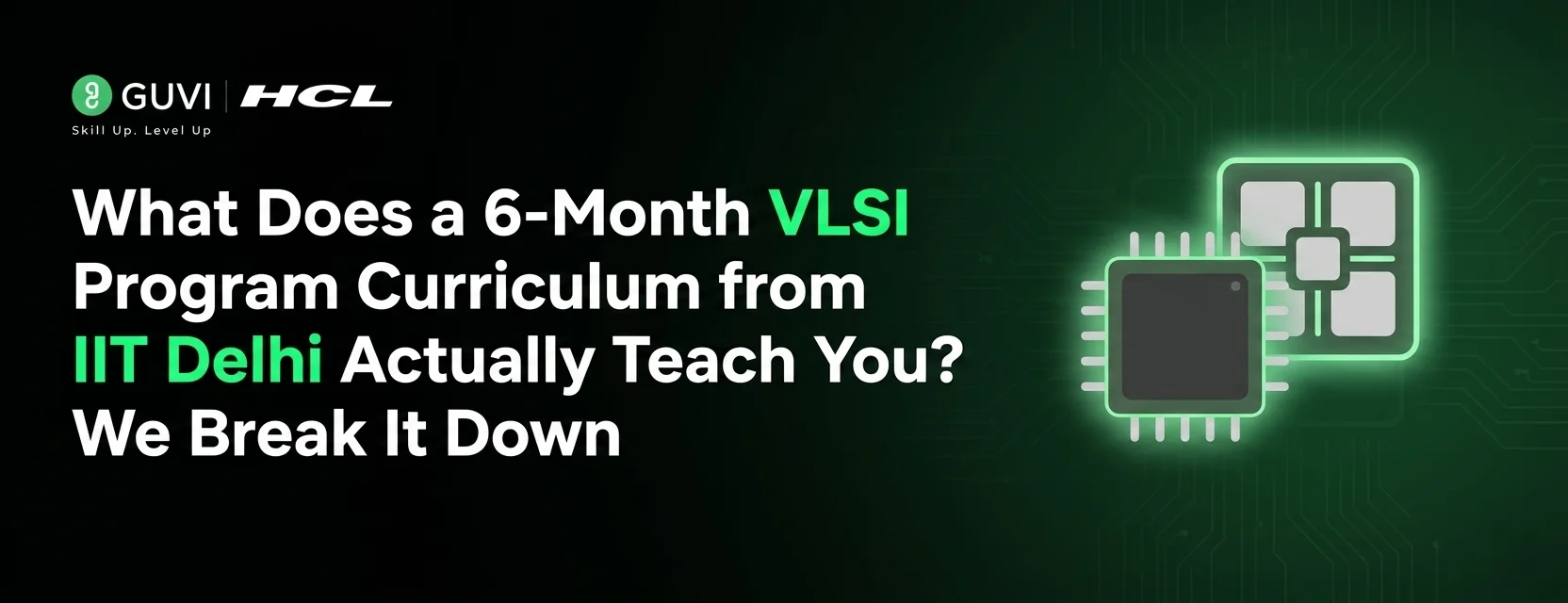
What Does a 6-Month VLSI Program Curriculum from IIT Delhi Actually Teach You? We Break It Down
Semiconductors Explained: A Complete Guide to Modern Technology(2026)
High-Paying Jobs for Diploma Students in Semiconductor Industry in India
HCL GUVI for VLSI Training: Master Chip Design and Verification with Industry-Aligned Course


Get In Touch For Details! Request More Information
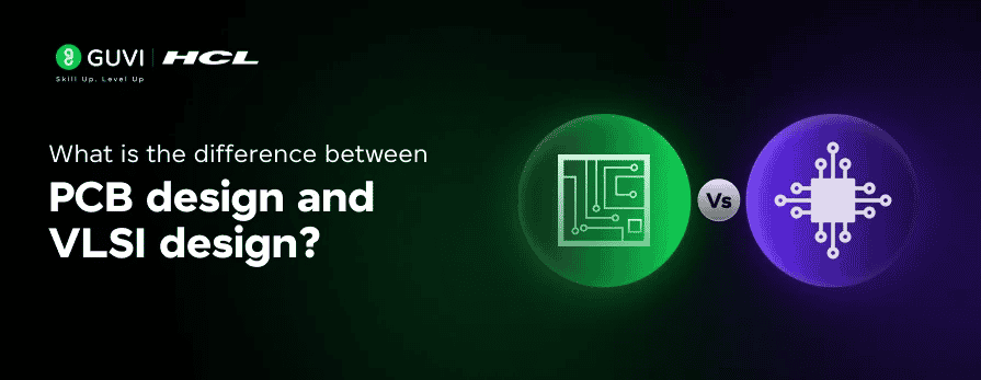
What is the Difference Between PCB Design and VLSI Design?
Jun 16, 2026 7 Min Read 6821 Views
(Last Updated)
Table of contents
- TL;DR:
- Real-World Examples: Where PCB & VLSI Design Live in Everyday Products
- PCB Design Process: Step-by-Step
- India’s Product-Led Chip Strategy
- AI-Automated Design Verification
- Chiplets, 3D ICs & 2nm Nodes
- Top PCB Design Trends in 2026
- AI Reduces Design Time by 40–60%
- AI-Driven Manufacturability Checks
- Digital Twins for Faster Validation
- Where is VLSI Design Used?
- Difference Between PCB Design and VLSI Design: Full Comparison Table
- Key Differences Between PCB Design and VLSI Design
- PCB Design Roles Focus On
- VLSI Design Roles Focus On
- PCB Design Career Growth Path
- VLSI Design Career Growth Path
- PCB Design vs VLSI Salary Comparison
- Which Should You Choose: PCB Design or VLSI Design?
- Choose PCB Design if you:
- Choose VLSI Design if you:
- Expert Recommendation for 2026
- Can a PCB Designer Switch to VLSI Design?
- Skills That Transfer from PCB to VLSI
- What You Need to Learn for the Transition
- Frequently Asked Questions
- What is the full form of PCB in VLSI?
- Is PCB and VLSI same?
- Is VLSI in ECE?
- Does VLSI have coding?
- What is VLSI language?
TL;DR:
- PCB design = board level; VLSI design = chip level
- PCB engineers connect pre-made chips on a circuit board; VLSI engineers design those chips
- PCB uses tools like Altium and KiCad; VLSI uses Cadence and Synopsys
- PCB requires minimal coding; VLSI requires Verilog or VHDL
- PCB is easier to learn and faster to get a job; VLSI has a steeper learning curve
- PCB prototyping costs ₹2,000 to ₹20,000; VLSI chip fabrication costs crores
- PCB salary in India: ₹3L to ₹25L; VLSI salary: ₹5L to ₹50L+
- PCB has wider job availability across electronics companies; VLSI is concentrated in semiconductor firms
- VLSI growth is explosive, driven by AI chips and India’s semiconductor mission; PCB demand remains stable
- Both are complementary; every electronic product needs both
For ECE students and engineers in India making career decisions in 2026, understanding these differences is not just academic; it is the foundation of choosing the right career path. India’s semiconductor industry is projected to create over 1 million jobs by 2026, making this one of the most important technology career choices of the decade.
This guide breaks down everything you need to know about the difference between PCB Design and VLSI Design, including clear definitions, tools, salary data, job roles, and a decision framework to help you choose the right path.
Real-World Examples: Where PCB & VLSI Design Live in Everyday Products
| Product / System | What the VLSI Engineer Builds | What the PCB Engineer Builds |
| Smartphone (iPhone 16 / Samsung Galaxy S25) | Designs the SoC, such as Apple A18 or Snapdragon 8 Gen 4, integrating CPU, GPU, AI engine, and 5G modem onto a 3nm chip with billions of transistors. Also develops LPDDR5 RAM and UFS storage ICs. | Designs the compact multilayer HDI motherboard that mounts the SoC, RAM, storage, RF modules, PMICs, and battery connectors while routing high-speed signals within a thin mobile form factor. |
| Electric Vehicle (Tata Nexon EV / Tesla Model 3) | Develops ADAS processors, motor control ASICs, and battery management ICs responsible for power flow and vehicle intelligence. | Designs Battery Management System boards, inverter control boards, onboard charger PCBs, and ADAS sensor boards capable of handling high voltage, thermal stress, and vibration. |
| AI Data Centre GPU (NVIDIA H100 / Google TPU v5) | Designs high-performance GPUs with advanced architectures, RTL, verification, physical design, and massive transistor integration for AI workloads. | Builds SXM5 carrier boards and high-layer-count server PCBs that manage extreme power delivery and ultra-high-speed interconnects between GPUs |
| Apple MacBook Pro (M4 Chip) | Develops the M4 SoC with multi-core CPU, GPU, and Neural Engine architecture on advanced process nodes. | Designs the ultra-compact multilayer logic board integrating the SoC, memory, storage, and Thunderbolt controllers in a very small space. |
| ISRO Satellite On-Board Computer | Designs radiation-hardened processors and memory chips capable of operating reliably in space environments. | Develops space-grade motherboards with polyimide substrates, conformal coatings, and redundant power systems built to survive launch and orbital conditions. |
Explore: VLSI Roadmap for beginners: 11 Steps to become a successful VLSI Engineer
1. What is PCB Design?
PCB (Printed Circuit Board) design is the process of creating the physical layout of a circuit board that mechanically supports and electrically connects electronic components, such as resistors, capacitors, microcontrollers, and integrated circuits, using conductive copper traces etched onto a non-conductive substrate.
The PCB acts as the physical backbone of virtually every electronic device.
Think of a PCB as the city map of an electronic device. Just as a city map defines roads (copper traces), plots (component pads), and neighbourhoods (functional zones), a PCB defines exactly how electrical current must flow between components to make the device work correctly.
Key Characteristics of PCB Design:
- Level of abstraction: Board-level (connects pre-manufactured components)
- Primary output: Gerber files for PCB manufacturing
- Core activity: Schematic capture, component placement, and trace routing
- Complexity range: Single-layer (simple gadgets) to 40+ layer boards (advanced computing systems)
- Key concerns: Signal integrity, thermal management, EMI/EMC compliance, Design for Manufacturability (DFM)

PCB Design Process: Step-by-Step
- Schematic Design: Create circuit blueprint using EDA tools
- Component Selection: Choose components based on specs, cost, and availability
- Board Layout: Define board size, layers, and place components
- Trace Routing: Connect components with copper traces (handle high-speed carefully)
- DRC Check: Ensure design meets manufacturing rules
- Gerber Files: Generate files for fabrication (Gerber, drill, BOM)
- Prototype & Test: Build, assemble, and validate the board
Where is PCB Design Used?
- Consumer Electronics: Smartphones, laptops, smart TVs, wearables
- Automotive Electronics: ECUs, ADAS systems, EV battery management systems
- Industrial Equipment: PLCs, motor controllers, industrial IoT sensors
- Aerospace and Defence: Avionics, radar, satellite communication systems
- Medical Devices: Patient monitors, imaging equipment, portable diagnostics
- Telecom and 5G: Base stations, routers, and antenna systems

What is VLSI Design?
VLSI (Very Large Scale Integration) design is the process of integrating millions or billions of transistors onto a single semiconductor chip (integrated circuit / IC) to perform complex computational functions. VLSI engineers design the microprocessors, memory chips, and custom ASICs (Application-Specific Integrated Circuits) that power modern computing, AI, 5G, and IoT devices.
If PCB design is the city map, then VLSI design is the construction of the buildings themselves, specifically designing the internal architecture, floor plans, and wiring of each structure at a microscopic level.
VLSI engineers work at the nanometre scale, designing structures that are thousands of times thinner than a human hair.
Key Characteristics of VLSI Design:
- Level of abstraction: Chip-level (designs the transistor-level circuitry inside ICs)
- Primary output: GDSII layout files for semiconductor fabrication (wafer manufacturing)
- Core activities: RTL coding, logic synthesis, physical design, timing analysis, DRC/LVS verification
- Languages used: Verilog, VHDL, SystemVerilog, Python (for automation)
- Key concerns: Power consumption, timing closure, area optimization, manufacturability at the nanometre scale
Explore: VLSI With No Coding Background: Cler 6 Month Career Blueprint
The VLSI Design Flow: Step by Step
Step 1: System Specification: Define what the chip must do, performance targets, power budget, area constraints, and application requirements.
Step 2: Architecture Design: Create a high-level blueprint of the chip’s functional blocks and how they communicate, data flow, interfaces, and sub-modules.
Step 3: RTL Coding: Write the hardware description in Verilog or VHDL, describing how data flows between registers and what operations occur at each clock cycle.
Step 4: Functional Simulation: Verify the RTL behaves correctly by running simulations against a testbench. Tools used: ModelSim, VCS, Xcelium.
Step 5: Logic Synthesis: Convert RTL code into a netlist of logic gates optimised for timing, area, and power. Tool: Synopsys Design Compiler.
Step 6: Physical Design (Place and Route): Place logic gates on the chip floor plan and route interconnects (wires) between them. Tools: Cadence Innovus, Synopsys ICC2.
Step 7: Timing and Power Analysis: Verify the chip meets timing requirements (STA) and power budgets across all operating conditions.
Step 8: Physical Verification: Run DRC (Design Rule Check) and LVS (Layout vs. Schematic) to confirm the layout matches the netlist and meets fab rules.
Step 9: Tapeout and Fabrication: Submit the final GDSII file to a semiconductor foundry (TSMC, Samsung, Intel Foundry) for wafer manufacturing.
Top VLSI Design Trend 2026
1. India’s Product-Led Chip Strategy
At VLSID 2026, India officially shifted from an assembly-focused approach to building indigenous silicon and domestic IP. The country is now targeting global semiconductor leadership by 2030.
2. AI-Automated Design Verification
Machine learning is transforming chip verification by identifying design flaws, optimising test coverage, and predicting issues earlier in the development cycle. This significantly reduces verification time and improves efficiency.
3. Chiplets, 3D ICs & 2nm Nodes
Demand is rapidly increasing for engineers skilled in heterogeneous integration, chiplet architectures, and advanced semiconductor nodes. Indian teams have already achieved 2nm tape-outs, with 3nm fabrication capabilities targeted by 2032. Expertise in TOP
Explore: India’s Semiconductor Mission: Opportunity for ECE and Engineering Students
Top PCB Design Trends in 2026
1. AI Reduces Design Time by 40–60%
AI-powered PCB layout tools can now automate routing, component placement, and stack-up recommendations across complex multilayer boards. Tasks that once required experienced engineers are becoming faster and more efficient, with some tools reporting over 90% auto-routing completion rates.
2. AI-Driven Manufacturability Checks
AI helps detect design flaws early in the process by improving signal integrity, thermal management, and board optimisation. This reduces costly redesigns and manufacturing rework.
3. Digital Twins for Faster Validation
AI-enabled digital twins simulate real-world operating conditions such as vibration, humidity, and thermal stress before fabrication begins. This reduces design risks and shortens product development cycles.
Where is VLSI Design Used?
- Smartphones: SoCs (Apple A-series, Qualcomm Snapdragon) integrate CPU, GPU, modem, and AI accelerator on one chip
- Artificial Intelligence: AI accelerator chips (NVIDIA H100, Google TPU) for training and inference
- 5G Infrastructure: Baseband processors, RF chips, and signal processors for 5G base stations
- Automotive: ADAS chips, EV motor control ICs, in-vehicle infotainment SoCs
- Data Centres: Server CPUs (AMD EPYC, Intel Xeon), memory controllers, networking ASICs
- Space and Defence: Radiation-hardened ICs for satellites and military electronics
Difference Between PCB Design and VLSI Design: Full Comparison Table
| Parameter | PCB Design | VLSI Design |
| Full Form | Printed Circuit Board Design | Very Large Scale Integration Design |
| What It Does | Designs the physical board connecting electronic components | Designs the integrated circuits (chips) placed on those boards |
| Level of Abstraction | Board-level | Chip-level |
| Analogy | City map defines roads and plots | Building construction designs the internal structure |
| Primary Tools | Altium Designer, KiCad, Eagle, OrCAD | Cadence, Synopsys, Mentor Graphics, HSPICE |
| Languages / Files | Gerber files, IPC standards | Verilog, VHDL, SystemVerilog, GDSII |
| Core Skills | Signal integrity, thermal management, DFM, EMC | Digital logic, RTL design, timing analysis, semiconductor physics |
| Coding Required? | Moderate to high | Yes, Verilog/VHDL for RTL design |
| Output | Physical circuit board | Silicon wafer (chip) |
| Complexity | Moderate to high | Very high |
| Prototyping Cost | ₹2,000–₹20,000 for a 4-layer prototype | ₹80L–₹8Cr+ for an ASIC mask set |
| Time to Prototype | Days to weeks | Months to years |
| Job Availability | Wide (any company making electronics) | Concentrated (semiconductor companies, EDA firms, fabless design houses) |
| Future Scope | Strong, driven by EV, IoT, 5G, PLI scheme | Explosive, driven by AI chips, 5G, India Semiconductor Mission |
| Interdependence | Uses VLSI-designed chips as components | Produces chips that PCB design integrates into complete systems |
PCB design and VLSI design are complementary. On a smartphone, the VLSI team designs the SoC chip, while the PCB team integrates it with the display, battery, and camera modules on the main board. Both disciplines are essential; they just operate at different levels.
Key Differences Between PCB Design and VLSI Design
PCB Design Roles Focus On
- PCB layout and routing
- Gerber generation
- Signal integrity basics
- Hardware debugging
- EMC/EMI compliance
- Manufacturing constraints
VLSI Design Roles Focus On
- Verilog/VHDL coding
- Chip verification
- Physical chip design
- Timing analysis
- ASIC/FPGA development
- Semiconductor workflows
PCB Design Career Growth Path
PCB Layout Designer → Hardware Engineer → Signal Integrity Engineer → PCB Design Lead → PCB Design Manager
VLSI Design Career Growth Path
RTL Engineer → Verification/Physical Design Engineer → ASIC Engineer → Senior Design Engineer → VLSI Architect / Design Manager
PCB Design vs VLSI Salary Comparison
| Career Path | Average Salary Range |
| PCB Design Roles | ₹3L – ₹15L |
| VLSI Design Roles | ₹6L – ₹30L |
VLSI engineers in India earn ₹6L–₹30L, with senior roles crossing ₹50L+. If that career path interests you, this is where to start.
Explore IT Delhi VLSI Design Course
Which Should You Choose: PCB Design or VLSI Design?
The honest answer is: it depends on your strengths, interests, and career goals. Here is a decision framework to help you think it through.
Choose PCB Design if you:
- Enjoy seeing tangible hardware results quickly and working with physical prototypes
- Want broader job availability across many industries, from startups to large manufacturers
- Prefer a lower entry barrier and a faster time to first employment after graduation
- Are interested in system-level hardware integration rather than chip-level design
- Want to work in automotive, IoT, EV, or consumer electronics manufacturing
- Prefer visual, layout-focused work over hardware coding
- Are interested in freelancing or working with product-stage hardware startups
Choose VLSI Design if you:
- Want the highest salary potential in hardware engineering, both in India and globally
- Enjoy logic design, hardware coding (Verilog/VHDL), and working at a high level of technical abstraction
- Are interested in chip design, AI hardware, or the semiconductor industry
- Want to work at companies like Intel, Qualcomm, NVIDIA, Texas Instruments, or India’s new semiconductor fabs
- Are willing to invest 4–6 months in focused upskilling through a structured training program
- Want to be at the centre of India’s semiconductor revolution driven by the ISM
- Have a strong foundation in digital electronics, number systems, and Boolean logic
Expert Recommendation for 2026
→ If you are an ECE or EEE fresher in India in 2026, VLSI design is the higher-return long-term investment. The India Semiconductor Mission, global AI chip demand, and the explosive growth of edge computing are creating a once-in-a-generation career opportunity. However, it requires genuine commitment to learning HDLs and EDA tools.
→ PCB design is an excellent, stable career choice with faster employment. especially in the EV, IoT, and electronics manufacturing sectors, being accelerated by India’s PLI scheme. The right choice depends on which kind of work excites you more.
Can a PCB Designer Switch to VLSI Design?
Yes, and this career transition is increasingly common in India’s growing semiconductor ecosystem. PCB designers have a genuine head start when moving to VLSI because they already understand hardware systems, signal flow, power distribution, and electronic component behaviour. These skills are directly valuable in VLSI, particularly in physical design and mixed-signal roles.
Skills That Transfer from PCB to VLSI
- Signal integrity knowledge maps directly to on-chip interconnect analysis and timing
- Power distribution experience is directly applicable to on-chip power delivery network (PDN) design
- Hardware debugging skills are valuable in VLSI verification and post-silicon debug
- Familiarity with EDA tool concepts accelerates VLSI tool learning significantly
- Understanding of component specifications and datasheets helps in IP block selection
What You Need to Learn for the Transition
Step 1: Digital Logic Design: Study combinational and sequential circuits, finite state machines (FSMs), timing diagrams, and Boolean algebra. This is the conceptual foundation of everything in VLSI.
Step 2: Hardware Description Languages: Learn Verilog (preferred for beginners) or VHDL. Practise writing, simulating, and debugging RTL code for basic to intermediate digital circuits.
Step 3: ASIC Design Flow: Understand the complete flow from RTL to GDSII, logic synthesis, place and route, static timing analysis, and physical verification. Know what each step does even before you become an expert in the tools.
Step 4: EDA Tools: Get hands-on practice with industry tools, Cadence for simulation and physical design, Synopsys for synthesis and STA. GUVI’s VLSI course provides access to these tools with guided labs.
Step 5: Semiconductor Physics Basics: Understand MOSFET operation, CMOS logic families, and basic fabrication concepts. You do not need a PhD, just enough to understand why design choices are made.
Step 6: Structured Training and Projects: Enrol in a recognised VLSI training program with real project work. Build at least one complete RTL-to-GDSII project to show employers.
Engineers who complete a structured VLSI training program typically transition within 4–6 months of focused learning and often achieve a 50–100% salary increase compared to their PCB design salaries.
If this guide helped you understand the difference between PCB design and VLSI design, the next step is clear. India’s semiconductor industry is growing fast, and the right training can put you ahead of 90% of applicants. Join the IIT Delhi VLSI Design Program
Frequently Asked Questions
1. What is the full form of PCB in VLSI?
PCB stands for Printed Circuit Board in VLSI, which is used for connecting and supporting electronic components in circuits.
2. Is PCB and VLSI same?
No, PCB (Printed Circuit Board) and VLSI (Very-Large-Scale Integration) are different. PCB is a physical board for connecting components, while VLSI refers to the process of integrating millions of transistors onto a single chip.
3. Is VLSI in ECE?
Yes, VLSI (Very-Large-Scale Integration) is a specialization within Electronics and Communication Engineering (ECE).
4. Does VLSI have coding?
Yes, VLSI design involves coding, typically in hardware description languages (HDLs) like VHDL or Verilog to design circuits.
5. What is VLSI language?
VLSI languages include VHDL (VHSIC Hardware Description Language) and Verilog, used for designing and modeling electronic systems.
Success Stories

About the Author
Salini Balasubramaniam
A curious, information-savvy writer loves to turn deep insights into authentic and engaging content that connects. With experience in writing for brands and driving audience engagement, I believe that words can make a powerful difference.
View all posts by Salini Balasubramaniam
Connect with me @


Did you enjoy this article?