


VLSI Design Articles
Why Chips Fail: A Basic Guide to Chip Defects and IC Failure Analysis
Fun Facts About the Semiconductor Industry
Why Are Semiconductor Chips Expensive? Manufacturing Cost Explained
Instruction Set Architecture: How ISA Shapes Modern Chip Design


Get In Touch For Details! Request More Information
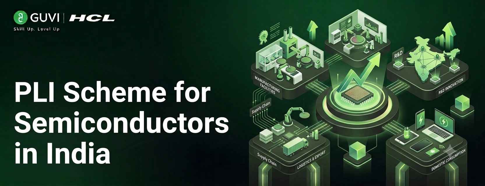
PLI Scheme for Semiconductors: India’s Chip Manufacturing Push Explained
Aug 06, 2026 7 Min Read 365 Views
(Last Updated)
Table of contents
- TL;DR Summary
- Introduction
- What is the PLI Scheme for Semiconductors?
- PLI Scheme for Semiconductors Meaning
- Why It Is Not Just One Scheme
- Why India Needs a Semiconductor PLI Scheme
- Strategic Importance of Chip Manufacturing in India
- Key Statistics You Should Know
- How India Semiconductor Policy Supports Chip Manufacturing in India
- India Semiconductor Policy Explained
- Role of India Semiconductor Mission
- Major Approved Project Categories
- Major Incentives Under the Semiconductor PLI Scheme
- Semiconductor Fab Incentives
- Design Linked Incentive Support
- ATMP and OSAT Support
- Semiconductor PLI Scheme vs Other Electronics Schemes
- Industry Impact and Career Opportunities
- Salary Snapshot for Semiconductor Careers in India
- Benefits of Creating an Indigenous Infrastructure For Semiconductor Push
- EV Industry: Smarter and More Reliable Electric Vehicles
- Telecom and 5G: Stronger Network Infrastructure
- Healthcare Devices: Affordable and Connected Medical Technology
- Defence and Aerospace: Secure and Mission-Critical Electronics
- Common Mistakes to Avoid While Understanding the Scheme
- Assuming the Scheme Only Supports Chip Fabs
- Thinking India Will Immediately Compete With Taiwan
- Confusing Electronics Assembly With Semiconductor Manufacturing
- Ignoring Skills Needed for Semiconductor Jobs
- Expecting Immediate Mass Hiring Across Every Role
- Wrapping Up
- Frequently Asked Questions
- What is the PLI Scheme for Semiconductors?
- Is the semiconductor PLI scheme the same as the Semicon India Programme?
- How much support does India provide for semiconductor fabs?
- Why is India's semiconductor policy important?
- What is ATMP in semiconductor manufacturing?
- Will chip manufacturing in India create jobs?
- Which skills are useful for semiconductor careers?
- Is VLSI a good career after the semiconductor PLI scheme?
- Does India already manufacture semiconductor chips?
- Who should learn about the PLI Scheme for Semiconductors?
TL;DR Summary
The PLI Scheme for Semiconductors is commonly used to describe India’s incentive-led push to build a domestic semiconductor ecosystem. Technically, it sits within the broader Semicon India Programme and India Semiconductor Mission, which support chip fabs, display fabs, compound semiconductors, ATMP/OSAT packaging units, and semiconductor design companies. India approved the original semiconductor programme with a ₹76,000 crore outlay in 2021, and Semicon 2.0 was approved in July 2026 to expand long-term support for design, manufacturing, materials, equipment, R&D, and talent.
Introduction
India does not want to remain only a consumer of chips. It wants to become a serious manufacturing and design hub for the chips that power smartphones, EVs, defence systems, data centres, medical devices, telecom networks, and AI hardware.
That is where the PLI Scheme for Semiconductors becomes important. In simple terms, it is India’s incentive-driven strategy to attract semiconductor investments, reduce import dependence, and build local capability across chip design, fabrication, assembly, testing, and packaging.
The scheme matters because semiconductor manufacturing is expensive, high-risk, and technology-intensive. A single fab can require billions of dollars, deep supply chains, skilled engineers, reliable power, water, cleanrooms, and long-term policy certainty.
What is the PLI Scheme for Semiconductors?
Before looking at investments and jobs, you need to understand one important point: India’s semiconductor push is broader than a usual production-linked incentive scheme.
Many people call it the semiconductor PLI (Production-Linked Incentive) scheme, but the official framework is the Semicon India Programme, implemented through the India Semiconductor Mission.
PLI Scheme for Semiconductors Meaning
The PLI Scheme for Semiconductors is an incentive framework designed to encourage companies to manufacture, package, test, and design chips in India.
Unlike regular PLI schemes that reward incremental production, the semiconductor programme offers capital support because chip fabs and packaging units require massive upfront investment.
The original Semicon India Programme was approved in December 2021 with an outlay of ₹76,000 crore for semiconductor and display manufacturing ecosystem development.
Why It Is Not Just One Scheme
India’s semiconductor policy combines multiple support mechanisms:
- Semiconductor fab incentives
- Display fab incentives
- Compound semiconductor support
- ATMP/OSAT packaging incentives
- Design Linked Incentive support
- Infrastructure support through semiconductor clusters
- Long-term ecosystem support under Semicon 2.0
This matters because chips are not made in one step. A company may design a chip in Bengaluru, fabricate wafers in Gujarat, package them in Assam, and test them for automotive or telecom use.
Why India Needs a Semiconductor PLI Scheme
India’s dependence on imported chips became a major concern during the global semiconductor shortage. Industries such as automobiles, consumer electronics, telecom, and medical devices faced delays because chips were not available on time.
The PLI Scheme for Semiconductors aims to reduce this vulnerability by building domestic capacity.
Strategic Importance of Chip Manufacturing in India
Chips are now strategic assets. They affect national security, industrial growth, digital infrastructure, and economic competitiveness.
For example:
- EVs need power semiconductors and microcontrollers.
- 5G equipment needs radio-frequency chips.
- AI servers need advanced processors and memory systems.
- Defence systems need reliable and secure electronics.
- Medical devices need embedded chips and sensors.
This is why chip manufacturing in India is not just an electronics story. It is a national capability story.
Key Statistics You Should Know
| Statistic | What It Means |
| ₹76,000 crore | Original Semicon India Programme outlay approved in 2021 |
| 50% project cost support | Fiscal support available for approved semiconductor fabs |
| 12 approved proposals | Approved semiconductor proposals under Semicon 1.0 as of July 2026 |
| ₹1.64 lakh crore | Cumulative investments linked to approved ISM projects |
| ₹1,27,500 crore | Fiscal outlay approved for Semicon 2.0 |
How India Semiconductor Policy Supports Chip Manufacturing in India
India’s semiconductor policy is designed to solve both investment and ecosystem challenges.
A fab alone cannot make India a semiconductor hub. The country also needs chip designers, materials suppliers, equipment support, testing labs, packaging units, skilled technicians, and VLSI engineers.
India Semiconductor Policy Explained
The India semiconductor policy focuses on building an end-to-end ecosystem.
That means India wants to support:
- Design
- Fabrication
- Assembly
- Testing
- Packaging
- Materials
- Equipment
- Research and development
- Talent development
Semicon 2.0, approved in July 2026, expands support beyond fabs to include areas such as chip design, materials, equipment, R&D, and talent development.
Role of India Semiconductor Mission
The India Semiconductor Mission acts as the nodal agency for appraising and recommending semiconductor projects.
It helps evaluate applications, coordinate policy support, and guide the long-term development of India’s semiconductor ecosystem.
According to official sources, the mission has helped move India from policy announcement to approved projects and early commercial production across selected units.
Major Approved Project Categories
India’s approved semiconductor projects include:
- Silicon fabs
- Compound semiconductor facilities
- ATMP units
- OSAT facilities
- Display-related semiconductor units
- Packaging facilities
This is a practical approach because India can enter the semiconductor value chain through multiple routes instead of waiting only for advanced-node fabs.
Major Incentives Under the Semiconductor PLI Scheme
The semiconductor PLI scheme works because it reduces financial risk for companies entering a capital-heavy industry.
Semiconductor manufacturing requires long gestation periods. Without government support, many companies may hesitate to invest.
Semiconductor Fab Incentives
For approved semiconductor fabs, the scheme provides fiscal support of up to 50% of the project cost on a pari-passu basis.
This means the government shares part of the capital burden with eligible companies.
Design Linked Incentive Support
Chip design is one of India’s strongest areas. Many global semiconductor companies already have large design centres in India.
The Design Linked Incentive scheme supports domestic companies, startups, and MSMEs in semiconductor design. It includes product design-linked incentives and deployment-linked incentives for eligible applicants.
ATMP and OSAT Support
ATMP and OSAT units focus on assembly, testing, marking, and packaging.
These facilities are crucial because they create a bridge between chip fabrication and final electronics manufacturing. They also require less capital than advanced fabs, making them a smart entry point for India.
A chip may look tiny, but making one is like building a microscopic city. It needs “roads” for electric signals, “buildings” called transistors, and ultra-clean factories where even a speck of dust can cause trouble.
Semiconductor PLI Scheme vs Other Electronics Schemes
India’s electronics manufacturing push includes several schemes. However, the PLI Scheme for Semiconductors is different because it supports deep-tech manufacturing, not just final product assembly.
| Scheme / Policy | Main Focus | Best Example | Why It Matters |
| Semiconductor Programme | Fabs, ATMP, OSAT, chip design | Semiconductor fabs and packaging units | Builds core chip ecosystem |
| Large Scale Electronics PLI | Electronics manufacturing | Mobile phone manufacturing | Boosts finished electronics output |
| IT Hardware PLI | Laptops, tablets, servers | IT hardware assembly | Reduces hardware import dependence |
| SPECS | Components and sub-assemblies | Electronic components | Supports supplier ecosystem |
| EMC 2.0 | Manufacturing clusters | Electronics parks | Provides infrastructure support |
Why This Difference Matters
A smartphone assembly plant and a chip fab are not the same.
Assembly creates scale and jobs quickly. Semiconductor manufacturing creates deeper strategic capability but takes more time, higher investment, and stronger technical talent.
That is why India needs both electronics PLI schemes and semiconductor-specific incentives.
Industry Impact and Career Opportunities
India’s semiconductor policy is already changing the career conversation for engineering students.
Earlier, many ECE, EEE, instrumentation, and physics graduates moved into generic IT roles because core electronics opportunities were limited. Now, chip design, verification, embedded systems, fabrication, and semiconductor packaging are becoming more visible career tracks.
Salary Snapshot for Semiconductor Careers in India
Glassdoor listings in 2026 show chip design and VLSI-related roles across companies such as Intel, Qualcomm, Texas Instruments, Arm, Wipro, and others with wide salary variation.
| Role | Beginner Range | Experienced Range | Skill Focus |
| VLSI Design Engineer | ₹4–10 LPA | ₹15–25+ LPA | RTL, Verilog, SystemVerilog |
| Chip Design Engineer | ₹6–12 LPA | ₹20+ LPA in top firms | ASIC, SoC, verification |
| Physical Design Engineer | ₹5–12 LPA | ₹18–30+ LPA | Timing, floorplanning, EDA tools |
| Embedded Systems Engineer | ₹4–9 LPA | ₹12–22 LPA | C, microcontrollers, RTOS |
| Semiconductor Test Engineer | ₹4–8 LPA | ₹10–18 LPA | validation, test automation |
Benefits of Creating an Indigenous Infrastructure For Semiconductor Push
The advantages for creating a robust semiconductor ecosystem via strategic policies such as the PLI Scheme for Semiconductors is not limited to chip factories or policy documents. Its real impact will be visible in industries that depend on reliable, affordable, and customized chips.
From EVs to telecom, healthcare, and defence, stronger local semiconductor capacity can help Indian companies reduce supply risks and design products for local market needs.
1. EV Industry: Smarter and More Reliable Electric Vehicles
An electric vehicle company needs battery management systems, power electronics, sensors, microcontrollers, and communication chips.

If India builds local semiconductor capacity, EV companies can reduce supply delays, customize chips for Indian road and weather conditions, and improve cost control.
For example, an Indian EV manufacturer can use locally designed chips to improve battery safety, charging efficiency, motor control, and vehicle diagnostics.
2. Telecom and 5G: Stronger Network Infrastructure
Telecom equipment requires RF chips, signal processors, power amplifiers, and network communication components.
Local semiconductor design and packaging can help India strengthen telecom infrastructure and reduce dependence on imported components.
This is especially important for 5G networks, where performance, latency, power efficiency, and secure communication hardware directly affect service quality.
3. Healthcare Devices: Affordable and Connected Medical Technology
Modern healthcare devices use chips for monitoring, sensing, imaging, diagnostics, and wireless connectivity.
With stronger chip manufacturing in India, companies can build more affordable devices such as portable ECG machines, glucose monitors, wearable health trackers, and remote patient monitoring tools.
This can support hospitals, clinics, and rural healthcare providers that need reliable medical technology at lower costs.
4. Defence and Aerospace: Secure and Mission-Critical Electronics
Defence and aerospace systems depend on secure, high-reliability chips for communication, radar, navigation, surveillance, drones, and control systems.
Local semiconductor capacity can help India reduce dependence on foreign suppliers for sensitive electronics.
For example, indigenously designed and packaged chips can support secure communication systems, unmanned aerial vehicles, and advanced defence electronics where supply-chain trust is critical.
Common Mistakes to Avoid While Understanding the Scheme
Many learners and professionals misunderstand the PLI Scheme for Semiconductors because headlines often simplify the policy. Here are the mistakes you should avoid.
1. Assuming the Scheme Only Supports Chip Fabs
A fab is important, but it is not the whole semiconductor ecosystem. India’s programme also supports ATMP, OSAT, compound semiconductors, display-related facilities, and chip design companies.
If you focus only on fabs, you may miss faster-growing career opportunities in packaging, testing, verification, embedded systems, and design automation.
For students, this is an important mindset shift. You do not need to work only inside a fab to build a semiconductor career.
Roles in VLSI design, design verification, DFT, validation, and embedded systems are equally relevant to the ecosystem.
2. Thinking India Will Immediately Compete With Taiwan
Semiconductor leadership takes decades. Taiwan, South Korea, Japan, the US, and the Netherlands have built their ecosystems over many years.
India’s current strategy is to enter the value chain through practical segments such as ATMP, OSAT, mature-node fabs, compound semiconductors, and design.
This does not mean India lacks ambition. It means the country is building capability step by step.
For learners, this is good news because ecosystem-building creates long-term career demand rather than one-time hiring spikes.
3. Confusing Electronics Assembly With Semiconductor Manufacturing
Electronics assembly means putting together finished products such as smartphones, laptops, or consumer devices.
Semiconductor manufacturing involves creating, processing, packaging, and testing chips that go inside those products.
Both are important, but semiconductor manufacturing is deeper, more technical, and more capital-intensive.
When you read about chip manufacturing in India, check whether the article is talking about wafer fabrication, packaging, testing, design, or final electronics assembly.
4. Ignoring Skills Needed for Semiconductor Jobs
Policy incentives can bring investment, but skilled talent turns investment into output.
Companies need engineers who understand digital electronics, Verilog, SystemVerilog, CMOS basics, timing analysis, semiconductor devices, embedded C, EDA tools, and testing workflows.
A degree alone may not be enough. You need project-based learning, tool exposure, and a portfolio that proves your ability.
This is especially true for VLSI roles, where recruiters often test fundamentals and practical design thinking.
5. Expecting Immediate Mass Hiring Across Every Role
Semiconductor projects have phases: approval, land, construction, cleanroom setup, equipment installation, pilot production, qualification, and commercial production.
Hiring also follows these phases. Design, construction, process, operations, packaging, testing, and maintenance roles may open at different times.
So, do not wait for one “perfect” hiring wave. Start building skills early and track which segment fits your background.
If you are from ECE, EEE, instrumentation, mechanical, chemical, materials science, or computer engineering, there may be different entry points into the semiconductor ecosystem.
If this semiconductor shift has made you curious about chip design careers, start building the fundamentals that hiring teams actually test: digital logic, Verilog, RTL design, verification, and VLSI workflows. A structured path such as the IIT-Delhi’s VLSI Design Program can help you move from interest to practical project-based readiness, along with access to an expert faculty, an interactive campus experience and placement assistance.
Wrapping Up
The PLI Scheme for Semiconductors is India’s attempt to build long-term strength in chip design, manufacturing, packaging, and testing. It is not a quick policy experiment. It is a strategic move to reduce import dependence, attract global investment, support domestic companies, and create skilled careers in VLSI, embedded systems, ATMP, and semiconductor engineering. For learners, the next step is clear: understand the ecosystem, choose a specialization, and start building hands-on semiconductor skills before the hiring curve becomes even more competitive.
Frequently Asked Questions
1. What is the PLI Scheme for Semiconductors?
The PLI Scheme for Semiconductors refers to India’s incentive-led semiconductor policy under the Semicon India Programme and India Semiconductor Mission. It supports fabs, ATMP/OSAT units, compound semiconductors, display fabs, and chip design companies.
2. Is the semiconductor PLI scheme the same as the Semicon India Programme?
Not exactly. People often use both terms interchangeably, but the official umbrella is the Semicon India Programme. The semiconductor PLI scheme is a common way to describe its incentive-based structure.
3. How much support does India provide for semiconductor fabs?
Approved semiconductor fabs can receive fiscal support of up to 50% of the project cost on a pari-passu basis, subject to eligibility and evaluation by the India Semiconductor Mission.
4. Why is India’s semiconductor policy important?
India semiconductor policy is important because chips power modern industries such as EVs, telecom, defence, AI, healthcare, and consumer electronics. Domestic capability can improve supply security and create high-skilled jobs.
5. What is ATMP in semiconductor manufacturing?
ATMP stands for Assembly, Testing, Marking, and Packaging. It is the stage where chips are packaged, tested, and prepared for use in electronic products.
6. Will chip manufacturing in India create jobs?
Yes. Chip manufacturing in India can create jobs in VLSI design, verification, embedded systems, process engineering, packaging, testing, equipment maintenance, materials, and production operations.
7. Which skills are useful for semiconductor careers?
Useful skills include digital electronics, Verilog, SystemVerilog, CMOS basics, RTL design, verification, timing analysis, embedded C, Linux basics, Python scripting, and EDA tool exposure.
8. Is VLSI a good career after the semiconductor PLI scheme?
Yes, VLSI is becoming more relevant as India expands chip design and manufacturing. Students with strong fundamentals and hands-on projects can explore roles in design, verification, DFT, physical design, and validation.
9. Does India already manufacture semiconductor chips?
India has approved multiple semiconductor projects and some companies have started commercial production under the mission, while larger fab and packaging projects are progressing in phases.
10. Who should learn about the PLI Scheme for Semiconductors?
Engineering students, electronics professionals, VLSI aspirants, policy learners, startup founders, and investors should understand the scheme because it shapes India’s future in electronics and deep-tech manufacturing.
Success Stories











Did you enjoy this article?