


VLSI Design Articles
Why Chips Fail: A Basic Guide to Chip Defects and IC Failure Analysis
Fun Facts About the Semiconductor Industry
Why Are Semiconductor Chips Expensive? Manufacturing Cost Explained
Instruction Set Architecture: How ISA Shapes Modern Chip Design

Get In Touch For Details! Request More Information
How to Become a VLSI Designer in 2026: Skills, Roadmap, Salary & Career Guide
Sep 08, 2026 10 Min Read 38474 Views
(Last Updated)
Table of contents
- TL;DR
- What is VLSI Design and Why is it Important?
- Core Components of VLSI Design
- How to Become a VLSI Designer in 2026
- Key Steps to Become a VLSI Designer
- Essential Educational Requirements To Become VLSI Designer
- Mastering the Basics To Become VLSI Designer
- Gain Skills Crucial for VLSI Designer
- Specialization Tracks
- Best VLSI Design Career Path in India 2026
- Build Your VLSI Design Portfolio
- Gain Practical Experience
- Career Paths and Salaries in VLSI Design
- Takeaways…
- FAQs
- What educational background is required to become a VLSI designer?
- What are the core technical skills needed for VLSI design?
- How can I gain practical experience in VLSI design?
- Is it possible to enter the VLSI field with just a bachelor's degree?
- What is the salary of a VLSI designer in India in 2026?
- Which VLSI domain is best for beginners?
- What skills are required to become a VLSI designer?
- How can I become a VLSI designer after engineering?
TL;DR
- VLSI design is the process of designing integrated circuits by combining millions or billions of transistors on a single chip.
- To become a VLSI designer in 2026, start with a strong foundation in digital electronics, analog electronics, semiconductor physics, and circuit design.
- Learn essential HDLs such as Verilog, SystemVerilog, or VHDL, along with the VLSI design flow, RTL design, verification, synthesis, physical design, and timing analysis.
- Gain hands-on experience with EDA tools, build practical VLSI projects, and create a portfolio that demonstrates your design and problem-solving skills.
- Choose a specialization such as front-end design, verification, physical design, analog/mixed-signal design, or SoC design based on your interests and strengths.
- A B.Tech/B.E. in ECE, EEE, CSE, or a related field is a common starting point, while an M.Tech or M.S. can help with advanced or specialized roles.
- In India, VLSI salaries vary significantly based on role, experience, specialization, company, and location, with specialized roles offering strong long-term earning potential.
Modern chips contain billions of transistors packed into spaces smaller than 10 nanometers. This showcases the incredible scale of Very-Large-Scale Integration (VLSI) technology that powers everything from your smartphone to advanced AI systems.
VLSI designers lead the creation of sophisticated integrated circuits that drive breakthroughs in automotive electronics, electric vehicles, and automation. The field offers exciting opportunities in an industry that remains notably resistant to automation.
A strong foundation in electrical engineering, expertise in hardware description languages, and practical experience with industry-standard tools will prepare you for VLSI design. This article outlines the steps, skills, and qualifications needed to start your career in VLSI design.
What is VLSI Design and Why is it Important?
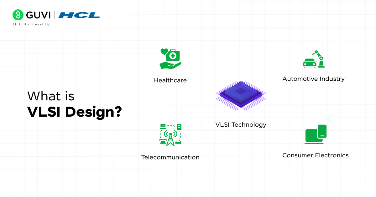
VLSI Design (Very Large Scale Integration) is the process of creating integrated circuits (ICs) by combining millions or even billions of transistors onto a single chip. It is a critical discipline in electronics engineering that involves designing and fabricating complex semiconductor devices used in modern electronic systems.
Core Components of VLSI Design
The process of designing VLSI circuits involves several critical components, each addressing a specific stage of development. These components collectively transform high-level functionality into a manufacturable integrated circuit. Here are five key components explained in detail:
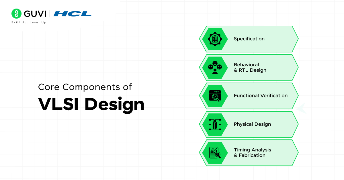
1. Specification
The design journey begins with a clear specification that outlines the chip’s requirements and constraints.
This stage defines what the circuit needs to achieve, including performance metrics like speed, power consumption, functionality, and physical size.
Specifications ensure that the design aligns with the product’s end-use and market demands, serving as a blueprint for subsequent stages.
2. Behavioral and RTL Design
Behavioral design involves defining the functionality of the circuit using high-level programming models, often in Hardware Description Languages (HDLs) such as Verilog or VHDL.
This phase focuses on how the circuit should behave under different inputs. It transitions into RTL (Register Transfer Level) Design, where the data flow between registers and logical operations is detailed.
RTL design bridges the gap between conceptual behavior and physical implementation, forming the backbone of the design process.
3. Functional Verification
Verification is critical to ensure the design works as intended before moving to physical implementation.
Functional verification involves simulating the HDL models to check for logical correctness, coverage, and compliance with the initial specifications.
Techniques such as simulation-based verification, formal verification, and assertion-based methods are employed. Without rigorous verification, undetected errors could lead to costly redesigns.
4. Physical Design
Physical design translates the verified logical representation into a physical layout that can be manufactured. This involves several stages:
- Floorplanning: Determining the placement of major functional blocks on the chip.
- Placement: Positioning individual cells or gates within blocks.
- Routing: Establishing interconnections between cells and blocks.
- Clock Tree Synthesis: Ensuring synchronized clock distribution. Each step optimizes the design for area, power, and performance while adhering to design rules.
5. Timing Analysis and Fabrication
Timing analysis ensures that all signal paths meet the required performance constraints, such as setup and hold times, to avoid errors during operation.
Tools like Static Timing Analysis (STA) identify potential bottlenecks. Once the timing is optimized, the design is sent for fabrication, where the physical chip is manufactured using advanced semiconductor processes.
Post-fabrication testing validates the chip’s real-world performance.
How to Become a VLSI Designer in 2026
Now we will discuss all the basics, technical skills, industry experience, and specializations you must gain to become a VLSI Designer.
Key Steps to Become a VLSI Designer
| Step | What to Learn | Tools/Technologies | Practical Outcome |
| 1. Build your electronics foundation | Digital logic, analog electronics, semiconductor physics | Digital/analog simulation tools | Strong understanding of circuits and devices |
| 2. Learn HDLs | Verilog, SystemVerilog, VHDL | HDL simulators | Ability to create RTL designs |
| 3. Understand the VLSI flow | RTL, synthesis, verification, physical design, STA | EDA tools | Understanding of RTL-to-GDSII workflow |
| 4. Choose a specialization | Front-end, verification, physical design, analog/mixed-signal, SoC | Domain-specific EDA tools | Career-focused technical skills |
| 5. Build projects | ASIC/FPGA, RTL, verification, physical design projects | Vivado, Yosys, Magic, commercial EDA tools | Portfolio evidence of practical skills |
| 6. Gain practical experience | Internships, labs, open-source projects | Linux, TCL, Python and EDA environments | Industry-oriented experience |
| 7. Prepare for VLSI roles | Resume, portfolio, interviews, core concepts | GitHub, LinkedIn and interview platforms | Job-ready VLSI profile |
Now we will discuss all the basics, technical skills, industry experience, and specializations you must gain to become a VLSI Designer, let’s get started.
Essential Educational Requirements To Become VLSI Designer
A strong educational foundation and ongoing learning are vital to build a successful career as a VLSI designer. Your journey starts with a bachelor’s degree in electrical engineering, computer engineering, or related fields.
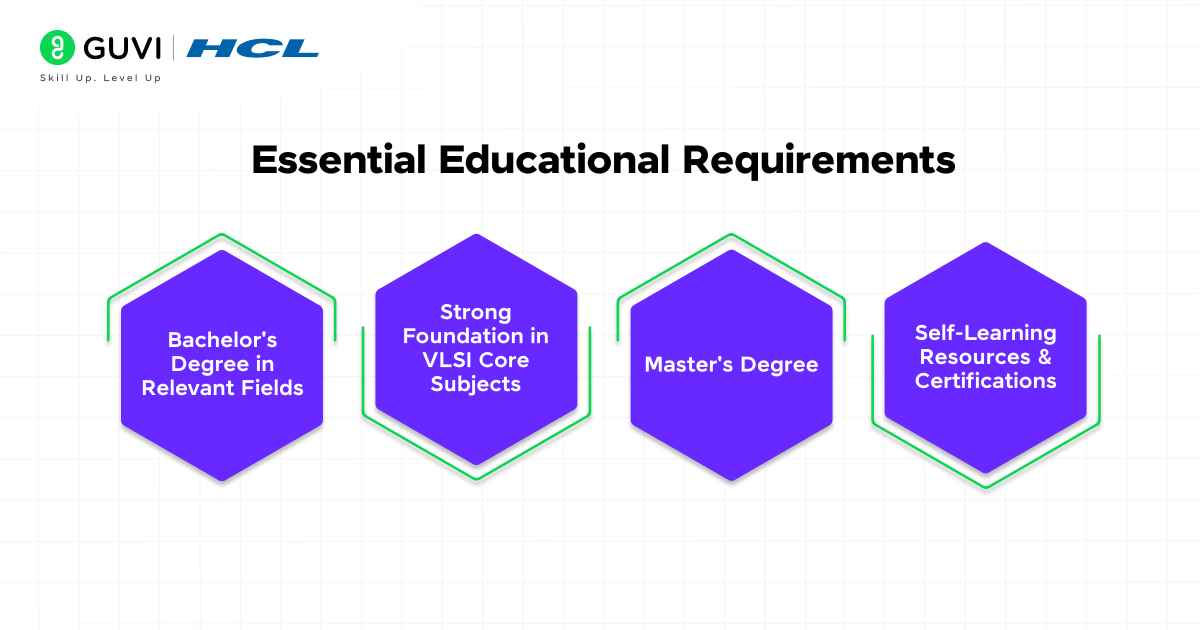
To embark on a successful career as a VLSI Designer, a strong educational foundation in electronics and related disciplines is critical. Below are the essential educational qualifications and knowledge areas necessary to excel in this field:
1. Bachelor’s Degree in Relevant Fields
- Requirement: A Bachelor of Technology (B.Tech) or Bachelor of Engineering (B.E.) in disciplines such as:
- Electronics and Communication Engineering (ECE)
- Electrical and Electronics Engineering (EEE)
- Computer Science Engineering (CSE) (for digital VLSI focus)
- Skills Acquired:
2. Strong Foundation in VLSI Core Subjects
During undergraduate studies, focusing on VLSI-related subjects is essential. These include:
- Digital Logic Design: Understanding logic gates, flip-flops, multiplexers, and sequential circuits.
- Analog Electronics: Fundamentals of transistors, op-amps, and analog circuit design.
- Semiconductor Physics: Knowledge of device physics, MOSFETs, and CMOS technology.
- Signals and Systems: Mathematical modeling of systems, signal processing, and transformations.
3. Master’s Degree (Optional but Recommended)
- While a bachelor’s degree is often sufficient for entry-level roles, pursuing a Master of Technology (M.Tech) or Master of Science (M.S.) will provide you with specialized knowledge and better career prospects.
- Specializations to consider:
- VLSI Design
- Microelectronics
- Embedded Systems
- Advanced coursework typically covers:
- Physical design automation
- High-level synthesis
- Advanced verification methodologies
- Low-power VLSI design
4. Self-Learning Resources and Certifications
To complement formal education, certifications and training programs are highly valuable:
Many platforms offer specialized VLSI training. The National Program on Technology Enhanced Learning (NPTEL) offers complete courses from top institutions.
These programs teach everything from digital circuits to FPGA programming. HCL GUVI, Coursera and edX platforms are great ways to learn Digital Systems and Logic Design that help understand processor design principles.
HCL GUVI’s VLSI Design and Verification Course is highly renowned in the industry for its expert-backed curriculum.
Intel and Micron’s industry-supported programs give you hands-on experience with real-life design challenges. Students learn synthesis, auto-place, and route methods to meet industry needs.
- VLSI Design Certifications from platforms like Cadence, Mentor Graphics, or Synopsys Purple.
- Courses on Hardware Description Languages (HDLs) such as Verilog and VHDL.
- Specialized programs in FPGA Design, ASIC Design, and EDA Tools.
Mastering the Basics To Become VLSI Designer
Mastering the basics is a critical step in laying a strong foundation for a career in VLSI design. Here are four essential steps to focus on, explained in detail:
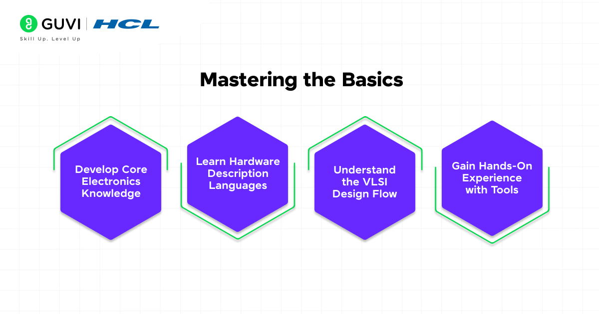
1. Develop Core Electronics Knowledge
A strong grasp of fundamental electronics principles is indispensable for understanding how integrated circuits (ICs) are built and function.
Begin with semiconductor physics, where you’ll learn how materials like silicon facilitate the creation of transistors, diodes, and other IC components.
Deepen your understanding of digital electronics, focusing on logic gates, multiplexers, and flip-flops, as these form the core of digital designs.
Additionally, gain insights into analog electronics for designing circuits like amplifiers and filters, which are essential in mixed-signal VLSI systems. Mastering these topics will ensure a solid theoretical base to tackle more advanced VLSI concepts.
2. Learn Hardware Description Languages
Hardware Description Languages (HDLs) like Verilog, VHDL, and SystemVerilog are the cornerstone of VLSI design.
These languages are used to describe the behavior and structure of electronic systems, enabling simulation and synthesis of complex digital circuits.
Start by learning to write and simulate basic combinational and sequential circuits. Move on to creating scalable designs with parameterization and modularity.
Understanding these HDLs will allow you to implement, verify, and debug digital systems effectively, aligning with industry standards and workflows.
3. Understand the VLSI Design Flow
The VLSI design process involves several critical stages, and understanding each is vital for success in this field.
Begin with specification, where system requirements are translated into design objectives. Progress to RTL design, using HDLs to define the functional behavior of the circuit.
Learn about logic synthesis, which converts RTL code into a gate-level representation, and physical design, where the circuit is mapped to silicon through placement and routing.
Finally, focus on verification and validation, ensuring the design meets functional and timing requirements. This knowledge provides a roadmap for transitioning from concept to a manufacturable chip.
4. Gain Hands-On Experience with Tools
Practical exposure is key to mastering VLSI design. Familiarize yourself with industry-standard EDA tools such as Synopsys, Cadence, and Mentor Graphics.
These tools are used for synthesis, simulation, verification, and physical design. Start by simulating simple circuits, gradually working on more complex designs.
Additionally, use tools like ModelSim for verification and Vivado for FPGA implementation.
By engaging in projects and competitions, you’ll develop the problem-solving skills needed to debug and optimize circuits. Hands-on practice bridges the gap between theoretical learning and industry applications.
Gain Skills Crucial for VLSI Designer
To become a successful VLSI Designer, you need to develop a combination of technical expertise and problem-solving skills. Here’s how you can build these:
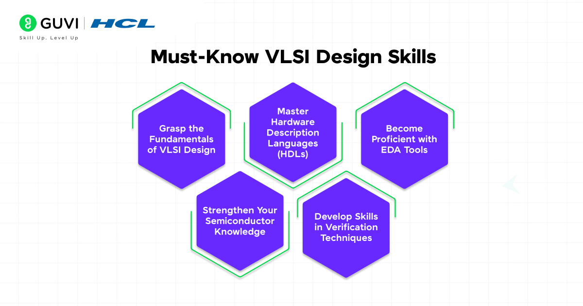
1. Grasp the Fundamentals of VLSI Design
To start, develop a strong understanding of digital logic design, microelectronics, and semiconductor physics.
These foundational concepts form the building blocks of VLSI. Learn about the VLSI design flow, including stages like synthesis, simulation, verification, and layout.
Familiarizing yourself with design types such as Application-Specific Integrated Circuits (ASICs) and Field-Programmable Gate Arrays (FPGAs) is also crucial, as they are the primary technologies used in modern VLSI.
2. Master Hardware Description Languages (HDLs)
As a VLSI designer, you’ll frequently use hardware description languages like Verilog and VHDL. These languages help you model and simulate digital circuits before physical implementation.
Focus on learning their syntax, semantics, and practical applications in creating Register-Transfer Level (RTL) designs.
By practicing extensively, you’ll gain the ability to describe circuits at both the behavioral and structural levels.
3. Become Proficient with EDA Tools
Electronic Design Automation (EDA) tools are essential for creating and testing VLSI designs. Gain hands-on experience with tools like Cadence Innovus, Synopsys Design Compiler, and Mentor Graphics Calibre.
These tools help you perform critical tasks like timing analysis, power optimization, and layout verification.
Being proficient in EDA tools gives you an edge in streamlining the design process and meeting industry standards.
4. Strengthen Your Semiconductor Knowledge
A deep understanding of semiconductor physics is fundamental to VLSI design.
Focus on learning how MOSFETs operate and their role in digital circuits. Explore concepts like threshold voltage, channel length modulation, and scaling.
Understanding these principles will enable you to design energy-efficient and high-performance chips, which are critical for modern electronics.
5. Develop Skills in Verification Techniques
Verification is an integral part of the VLSI design process. You’ll need to ensure that your designs function as intended.
Learn about functional verification, static timing analysis (STA), and formal verification techniques.
Additionally, gaining familiarity with advanced verification methodologies such as Universal Verification Methodology (UVM) will enhance your ability to test complex designs effectively.
Specialization Tracks
When entering the VLSI field, specializing in a particular domain is essential to align your career with your interests and strengths.
Each specialization not only comes with unique responsibilities but also offers competitive salaries based on expertise. Let’s discuss them:
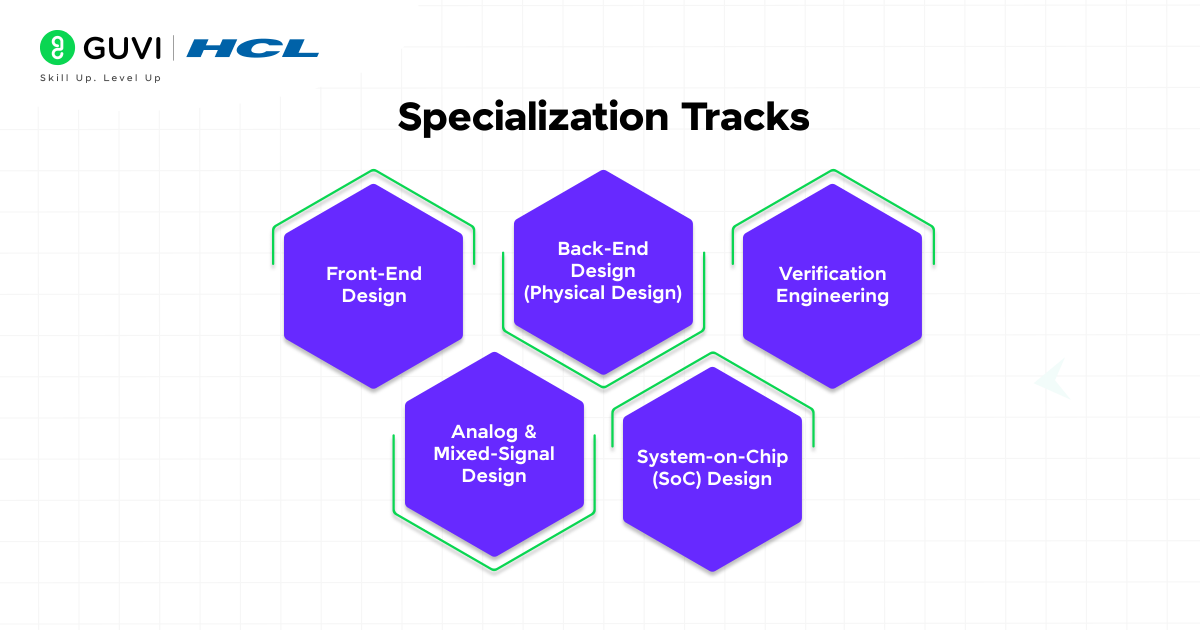
1. Front-End Design
Front-end design focuses on developing the logical and functional aspects of a chip.
Your responsibilities include designing architecture, writing code in hardware description languages (HDLs) like Verilog or VHDL, and conducting simulations to ensure functional correctness.
Responsibilities: Logic design, RTL coding, simulation, and collaboration with verification engineers.
Average Salary: ₹12.7–14 LPA for freshers; ₹13.9-18.7 LPA for experienced professionals (5+ years).
2. Back-End Design (Physical Design)
The physical design transforms the logical design into a physical layout.
This process includes component placement, routing, timing analysis, and power optimization. Your work ensures the chip meets manufacturability and performance goals.
Responsibilities: Placement, routing, timing closure, signal integrity analysis, and thermal management.

Average Salary: ₹14.8-16.3 LPA for entry-level engineers; ₹29.5–32.6 LPA for senior roles.
3. Verification Engineering
Verification engineers ensure the logical design functions as intended.
Using tools and methodologies like UVM (Universal Verification Methodology), you will test and debug designs through exhaustive simulation and analysis.
Responsibilities: Testbench creation, functional and formal verification, debugging, and ensuring design quality.
Average Salary: ₹13.5–14.9 LPA for freshers; ₹20.1–22.3 LPA for senior roles.
4. Analog and Mixed-Signal Design
This specialization involves designing analog circuits and components such as amplifiers, oscillators, and data converters.
The mixed-signal design integrates analog and digital blocks, requiring a deep understanding of both domains.
Responsibilities: Circuit design, performance optimization, and validation of mixed-signal systems.
Average Salary: ₹7.6-8.4 LPA for entry-level engineers; ₹7–9.3 LPA for experts.
5. System-on-Chip (SoC) Design
SoC design integrates multiple functionalities like processors, memory, and peripherals into a single chip. It requires expertise in both hardware and software.
Responsibilities: IP integration, power management, clock synchronization, and system-level performance optimization.
Average Salary: ₹18.7–20.7 LPA for freshers; ₹21–25.5 LPA for senior roles.
Best VLSI Design Career Path in India 2026
The best VLSI career path in India in 2026 depends on your background, interests, and the part of the chip-design flow you enjoy most.
Rather than trying to master every VLSI domain at once, choose one specialization and build depth in its core skills.
| VLSI Career Path | Best Suited For | Core Skills to Build | Key Technologies/Tools |
| RTL/Front-End Design | Students who enjoy digital logic and coding | Digital design, RTL, Verilog/SystemVerilog | Verilog, SystemVerilog, synthesis tools |
| Design Verification | Those who enjoy debugging and testing | Verification, assertions, testbenches, UVM | SystemVerilog, UVM, simulation tools |
| Physical Design | Students interested in chip implementation | Floorplanning, placement, routing, STA | Cadence Innovus, Synopsys implementation tools |
| Analog/Mixed-Signal | Students interested in circuit-level design | Analog circuits, CMOS, semiconductor devices | Analog IC design and simulation tools |
| SoC Design | Engineers interested in complete chip systems | Architecture, IP integration, interfaces, power | SoC/RTL/verification environments |
For beginners, front-end RTL design and verification can provide a structured starting point because they build directly on digital logic and HDL fundamentals.
However, physical design, analog design, and SoC roles can also be strong career paths once you have the required foundation.
In 2026, learning should also include practical exposure to current EDA workflows rather than focusing only on theory.
Cadence’s Innovus 25.1 is used for modern implementation workflows, while Synopsys Design Compiler NXT is positioned for next-generation RTL synthesis and advanced process-node requirements.
Build Your VLSI Design Portfolio
A strong portfolio helps you stand out in the competitive VLSI design industry.
Your carefully chosen projects and proper documentation show potential employers your technical expertise and problem-solving abilities.
Personal Projects to Showcase
Your portfolio should highlight projects that show your understanding of the physical design flow. Choose projects that match what the industry needs and display your expertise in:
- VLSI circuit design and simulation
- Temperature sensor implementations
- Bandgap reference designs
- SPI/I2C protocols
- Neural network processing units
- Automated ASIC design flows
We focused on projects that show breakthroughs or optimizations you created.
To cite an instance, contributing to open-source VLSI projects lets you work with experienced engineers and displays your problem-solving skills on public platforms.
GitHub Repository Setup
A well-organized repository boosts your portfolio’s professional appeal.
Create a well-laid-out project directory that has RTL designs, simulation results, and implementation details.
Keep separate branches for development and stable releases during setup.
Your repository should clearly show how well you understand automated RTL-to-GDSII flows, open-source tools like Yosys and Magic, and design exploration capabilities.
Add detailed README files that explain your project’s goals, implementation methods, and results alongside your code.
Documentation Best Practices
Documentation proves your capabilities and achievements. Your documentation should have:
Design specifications and objectives, Implementation methodology, Tools and techniques employed, Performance metrics and results, Effects of your contributions
Ask professionals or mentors in the field to review your documentation’s content and presentation. Combine all your work in one available location through LinkedIn and personal websites.
This makes it easier for potential employers to review your skills.
Gain Practical Experience
Hands-on experience is a vital stepping stone to becoming a successful VLSI designer. You’ll build expertise in this ever-changing field through hands-on exposure and professional development.
Internship Opportunities
The VLSI industry offers many internship positions in leading semiconductor companies.
Major organizations like NVIDIA, Intel, AMD, and Synopsys recruit interns for various roles, including ASIC design, verification, and physical design. These positions help students learn about chip design, validation, and implementation.
Look beyond traditional roles and explore specialized internships in:
- Product validation engineering
- Hardware verification
- ASIC implementation
- Physical design
- Architecture development
Industry Certifications
Synopsys Purple Certification Program provides complete training for final-year students and fresh graduates. This program features five specialized tracks:
- Physical Design
- Design Verification
- RTL Synthesis
- Design for Test
- Analog Mixed Signal Circuit and Layout Design
Note that proficiency in simple programming skills like Linux, TCL/TK, Perl, and Python is essential. These programs help you master industry-standard tools and methodologies that make you more competitive in the job market.
Career Paths and Salaries in VLSI Design
The semiconductor industry is growing faster than ever, which creates many career opportunities for VLSI designers.
The field offers excellent growth potential and competitive compensation, from entry-level positions to specialized roles. Below are the key career paths along with their commendable salaries:
1. Front-End VLSI Roles
- RTL (Register Transfer Level) Designer: As an RTL Designer, you’ll create digital circuits using hardware description languages (HDLs) like Verilog or VHDL. Entry-level salaries typically range from ₹10.5-11.6 LPA. With experience, mid-level RTL Designers can expect salaries between ₹7.7-11.4 LPA.
- Functional Verification Engineer: These engineers test and verify the functionality of digital designs. For entry-level professionals, salaries start at ₹25.2-27.9 LPA. Experienced verification engineers can earn between ₹37.2–38 LPA.
- Emulation Engineer: Emulation Engineers validate designs in hardware models to find design flaws before fabrication. Entry-level salaries start at ₹19.8–26.7 LPA, while mid-level roles can go up to ₹17.6–38.8 LPA.
2. Back-End VLSI Roles
- Physical Design Engineer: This role focuses on converting logical designs into physical chip layouts, ensuring proper placement, routing, and timing closure. Entry-level salaries range from ₹6.8–8.1 LPA. Experienced engineers typically earn between ₹6.3–10.6 LPA, depending on their expertise.
- Design for Testability (DFT) Engineer: DFT Engineers design methodologies to ensure that chips are testable after fabrication. These engineers typically earn ₹14.5-16.2 LPA at entry-level positions, and senior roles can command salaries from ₹16.4–28.6 LPA
3. Specialized VLSI Roles
- Analog Design Engineer: Analog Design Engineers focus on creating analog circuits, such as amplifiers and data converters. For entry-level positions, salaries typically range from ₹17.5-19.3 LPA, with experienced engineers earning between ₹15.9–21.1 LPA.
- RF (Radio Frequency) Engineer: RF Engineers design circuits for high-frequency wireless communication. They usually earn ₹4.2-4.6 LPA at entry-level and can see their salary grow to ₹7-13.4 LPA with experience.
- EDA Tools Engineer: These engineers work on the development and enhancement of Electronic Design Automation (EDA) tools. Entry-level salaries range from ₹9.1-10.1 LPA, while senior EDA engineers can expect ₹10–20+ LPA.
4. System-Level Roles
- SoC (System-on-Chip) Architect: SoC Architects design chips that integrate various functionalities into a single unit. In India, salaries for mid-level SoC Architects range from ₹18.7–20.7 LPA, and senior-level professionals can earn ₹21-25.5 LPA or more, depending on their experience.
- Hardware System Engineer: These engineers focus on integrating VLSI designs into larger systems. Freshers can expect ₹8.4-9.3 LPA, while experienced system engineers earn ₹9.3-10.8 LPA.
The salaries in VLSI Design can vary depending on the specialization, company, and experience level.
As a rule of thumb, professionals in specialized areas like RF design or SoC architecture tend to earn higher salaries due to the advanced expertise required.
Takeaways…
VLSI design is the lifeblood of modern technological advancement that powers everything from smartphones to autonomous vehicles.
The path to becoming a VLSI designer needs dedication to master both fundamental concepts and specialized skills in digital, analog, or mixed-signal design.
Personal projects, internships, and industry certifications will set you apart in this competitive field, rather than just theoretical knowledge.
Your portfolio will be tangible proof of your expertise and shows you know how to handle complex circuit designs and create efficient solutions.
The VLSI industry provides remarkable career growth opportunities with salaries ranging from ₹10-50 LPA.
I hope this article has aided your learning journey and if you have any doubts or feedback to share, reach out to me through the comments section below.
FAQs
1. What educational background is required to become a VLSI designer?
A B.Tech or B.E. degree in Electronics and Communication Engineering (ECE), Electrical and Electronics Engineering (EEE), Computer Science Engineering (CSE), or a related field is a common starting point for a VLSI career. You should also have a strong foundation in digital logic, analog electronics, semiconductor physics, and basic programming. A master’s degree in VLSI Design, Microelectronics, or a related specialization can be useful for advanced roles.
2. What are the core technical skills needed for VLSI design?
Essential skills include proficiency in hardware description languages (like Verilog and VHDL), expertise in Electronic Design Automation (EDA) tools, and a strong understanding of digital and analog circuit design principles.
3. How can I gain practical experience in VLSI design?
You can gain practical experience through internships at semiconductor companies, working on personal projects, participating in open-source VLSI projects, and pursuing industry certifications like the Synopsys Purple Certification Program.
4. Is it possible to enter the VLSI field with just a bachelor’s degree?
Yes, it’s possible to enter the VLSI field with a bachelor’s degree, especially for roles in design verification and validation. However, advanced positions and research roles often require higher degrees. Building a strong portfolio of projects and gaining practical experience can significantly boost your chances of landing a job with a bachelor’s degree.
5. What is the salary of a VLSI designer in India in 2026?
VLSI salaries in India vary based on experience, specialization, company, location, and technical skills.
Entry-level roles can start at different salary levels depending on the position, while experienced professionals in specialized areas such as analog design, RF, physical design, and SoC architecture can earn substantially more.
6. Which VLSI domain is best for beginners?
There is no single VLSI domain that is best for everyone.
* Front-end design and verification can be good starting points for beginners who enjoy digital logic and coding because they allow you to build on HDL and RTL fundamentals.
* Learners interested in chip implementation can explore physical design, while those interested in transistor-level circuits can consider analog and mixed-signal design.
Choosing a specialization based on your interests and strengths can make the learning process more manageable.
7. What skills are required to become a VLSI designer?
The key skills required include:
Digital logic and circuit design
Analog electronics
Semiconductor physics
Verilog, SystemVerilog, or VHDL
RTL design
VLSI design flow
Functional verification
Static Timing Analysis (STA)
EDA tools
ASIC and FPGA concepts
Linux and scripting
Python and TCL
The exact skills depend on your chosen specialization. For example, verification roles require strong testing and debugging skills, while physical design roles require knowledge of placement, routing, timing closure, and related implementation concepts.
8. How can I become a VLSI designer after engineering?
After engineering, start by strengthening your digital electronics, semiconductor, and VLSI fundamentals. Next, learn hardware description languages such as Verilog, SystemVerilog, or VHDL, understand the VLSI design flow, and gain hands-on experience with EDA tools.
You should then choose a specialization such as front-end design, verification, physical design, analog/mixed-signal design, or SoC design. Building practical projects, completing internships, and developing a portfolio can help you demonstrate your skills to employers.
Success Stories

About the Author
Hashmithaa
Hi, I’m Hashmithaa — a content writer with a love for words. Writing isn’t just what I do; it’s how I connect, communicate, and create meaning in a noisy digital world. And if my words help someone make a better decision, learn something new, or feel more confident, then I’ve done my job well.
View all posts by Hashmithaa
Connect with me @

Did you enjoy this article?
Comments













Very good and usefull
Yes Iam from ECE ,i learnt so many things and basis about VSLI . Thankyou ❤️
Thankyou for sharing this wonderful content 🙂
Well written!