


VLSI Design Articles
Why Chips Fail: A Basic Guide to Chip Defects and IC Failure Analysis
Fun Facts About the Semiconductor Industry
Why Are Semiconductor Chips Expensive? Manufacturing Cost Explained
Instruction Set Architecture: How ISA Shapes Modern Chip Design

Get In Touch For Details! Request More Information
What is VLSI Design? Career Scope, Salary & How to Start in 2026
Jul 22, 2026 7 Min Read 17337 Views
(Last Updated)
Imagine a world where your smartphone fits in your pocket, your smartwatch tracks your health seamlessly, and your laptop delivers lightning-fast performance, all while being incredibly compact and mobile.
The magic behind this incredible technology lies in a revolutionary technology called Very Large Scale Integration (VLSI). VLSI design is the art and science of packing millions or even billions of transistors onto a tiny silicon chip, enabling the creation of high-performance, energy-efficient, and compact devices that power our modern lives.
VLSI design plays a pivotal role in shaping the technology we rely on every day. Let’s dig deeper into the fascinating world of VLSI, exploring its process, applications, and the promising career opportunities it offers.
Table of contents
- TL;DR Summary
- VLSI: The Basics
- How Does VLSI Design Work?
- Specification
- Design Architecture
- Logical Design
- Circuit Design
- Physical Design
- Fabrication
- Testing and Validation
- Packaging and Deployment
- Applications of VLSI in India
- VLSI vs Embedded Systems - Which is Better for Career?
- Career Paths in VLSI
- Front-End Design Engineer
- Back-End Design Engineer
- Verification Engineer
- Analog Design Engineer
- FPGA Design Engineer
- Embedded Systems Engineer
- Semiconductor Process Engineer
- Salary of VLSI Designers in India
- VLSI Job Roles, Salary, Skills & Hiring Companies at a Glance
- Is VLSI a Good Career in 2026?
- Required Skills for a Career in VLSI
- Getting Started with VLSI Design
- Conclusion
- FAQs
- What is VLSI Design?
- What is the scope of VLSI in India?
- What is the average salary of a VLSI Design Engineer in India?
- Which companies in India hire VLSI professionals?
- What skills are essential for a career in VLSI design?
TL;DR Summary
- VLSI stands for Very Large Scale Integration: packing millions or billions of transistors onto a single chip.
- The design flow runs from specification and architecture through logical design, circuit design, physical design, fabrication, testing, and packaging.
- India’s VLSI applications span consumer electronics, automotive, telecom, and healthcare, backed by government initiatives like the ESDM push.
- VLSI vs embedded systems comes down to chip-level design work versus hardware-software integration; both offer strong career ceilings.
- Career paths range from front-end and back-end design to verification, analog, FPGA, embedded systems, and process engineering, with salaries from ₹1.8 lakh to ₹37+ lakh per annum depending on experience.
- Job-openings data through 2026 points to a genuine, structural shortage of skilled VLSI engineers in India, not a short-term spike.
VLSI: The Basics
The full form of VLSI is Very Large Scale Integration, a process used in electronics to create integrated circuits (ICs) by combining millions (or even billions!) of transistors onto a single chip. Essentially, it’s the backbone of modern electronic devices.
Before VLSI, circuits were built using large, bulky components. These were fine for basic tasks, but as technology advanced, the demand for smaller, faster, and more efficient systems grew.
VLSI stepped in to meet this demand by miniaturizing components and making chips more powerful and versatile.
Discover: How to Learn a VLSI Course from Scratch? 12 Steps To Follow
How Does VLSI Design Work?
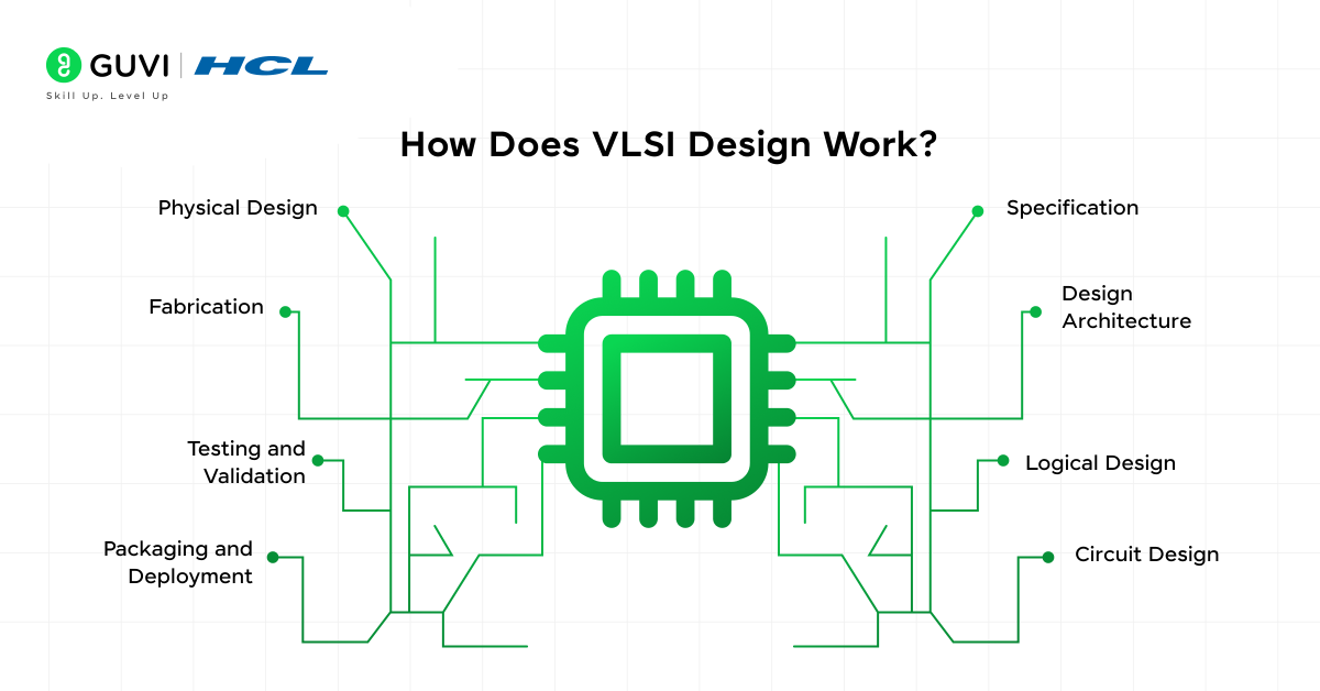
The process of VLSI (Very Large Scale Integration) design is a fascinating and intricate journey that transforms an idea into a functioning silicon chip. It involves multiple stages, each contributing to the creation of compact, efficient, and high-performance integrated circuits (ICs).
Here’s a detailed look at how VLSI design works:
1. Specification
Every chip begins with a clear purpose. The specification stage defines the goals, functionalities, and performance requirements of the chip.
This includes factors like processing speed, power consumption, area constraints, and the specific tasks the chip needs to perform. For example, is it a chip for a smartphone’s processor or an AI accelerator? Specifications serve as a blueprint for all subsequent stages.
2. Design Architecture
Once the specifications are defined, the architecture stage outlines the overall structure of the chip. This is where engineers decide how the chip will function at a high level.
They determine the components it will include, such as processors, memory units, communication buses, and interfaces, and how these components will interact.
The architecture acts as a roadmap, ensuring all components work together seamlessly to achieve the desired functionality.
3. Logical Design
At this stage, engineers dive into the logical representation of the chip. They use hardware description languages (HDLs) like Verilog or VHDL to describe the chip’s behavior.
This is similar to coding software, but instead of programming a computer, engineers are defining how the hardware will behave.
For example, they might define how a processor fetches, decodes, and executes instructions or how data flows through a memory subsystem. Simulation tools are used extensively here to verify the logic and identify errors.
4. Circuit Design
The circuit design stage translates the logical design into an actual electronic circuit. Engineers select the types of transistors, logic gates, and other components to implement the desired behavior. They optimize the circuit for performance, power efficiency, and reliability.
At this stage, factors like signal timing, voltage levels, and noise immunity are carefully analyzed to ensure the circuit operates correctly in real-world conditions.
5. Physical Design
The physical design stage is where the logical blueprint becomes a tangible layout on a silicon chip. It involves several key steps:
- Placement: Determining where each component (e.g., logic gates, transistors) will physically reside on the chip.
- Routing: Connecting these components with metal wires to allow communication.
- Optimization: Adjusting the layout to minimize delays, power consumption, and chip area while maximizing performance.
Engineers use specialized CAD (like Cadence or Synopsys) to perform these tasks. The final output of this stage is a detailed layout file that guides the chip fabrication process.
6. Fabrication
With the design finalized, the chip moves to the fabrication stage, which takes place in a semiconductor foundry. Here’s how it works:
- A silicon wafer is prepared as the base material.
- Photolithography, etching, and deposition techniques are used to layer the circuits onto the wafer.
- Transistors, interconnects, and other components are built layer by layer, creating the integrated circuit.
This stage requires extreme precision, as the smallest misalignment can render the chip non-functional.
7. Testing and Validation
Once the chip is fabricated, it undergoes rigorous testing and validation. This ensures that the chip performs as intended and meets the original specifications. Testing includes:
- Functional Testing: Verifying the chip’s logical operations.
- Performance Testing: Checking parameters like speed, power consumption, and thermal stability.
- Stress Testing: Evaluating how the chip performs under extreme conditions.
Any errors or defects identified during testing are analyzed, and the design may be revised to address them before mass production.
8. Packaging and Deployment
After successful validation, the chip is packaged to protect it from physical damage and facilitate its connection to external components. The packaged chips are then integrated into devices like smartphones, computers, cars, or other systems.
The VLSI design process is a blend of creativity, engineering, and cutting-edge technology. It involves a meticulous journey from defining what a chip will do to physically manufacturing it.
Explore: What are the 5 Levels in VLSI Design?
Applications of VLSI in India
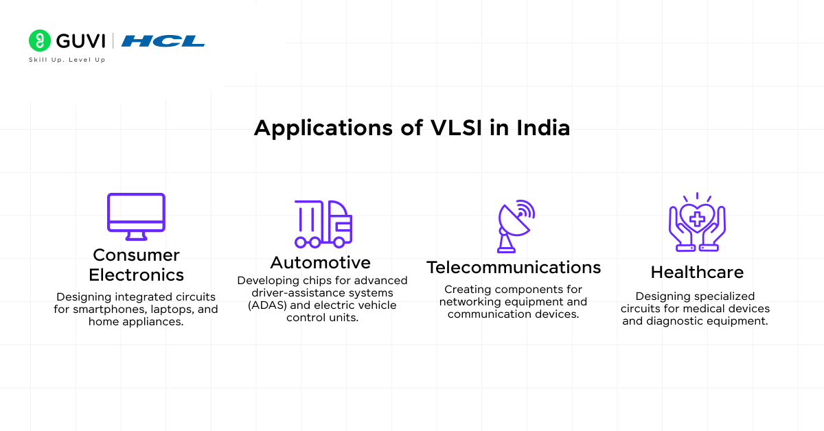
India’s electronics and semiconductor sectors are expanding rapidly, driven by increasing demand for digital devices and electronic goods. The Ministry of Electronics and IT anticipates that India’s semiconductor consumption will rise to $70–80 billion by 2026.
This growth is creating a substantial demand for skilled VLSI professionals across various industries, including:
- Consumer Electronics: Designing integrated circuits for smartphones, laptops, and home appliances.
- Automotive: Developing chips for advanced driver-assistance systems (ADAS) and electric vehicle control units.
- Telecommunications: Creating components for networking equipment and communication devices.
- Healthcare: Designing specialized circuits for medical devices and diagnostic equipment.
The Indian government’s initiatives, such as allowing 100% FDI in the Electronics System Design and Manufacturing (ESDM) sector and establishing the Electronics Development Fund (EDF), further bolster the VLSI industry’s growth.
Also Read: Types of VLSI Design: A Practical Guide for Beginners [2026]
VLSI vs Embedded Systems – Which is Better for Career?
Students exploring core electronics careers often get stuck choosing between VLSI design and embedded systems. Both fields deal with hardware, but they solve very different problems and suit different kinds of engineers.
| Factor | VLSI Design | Embedded Systems |
|---|---|---|
| What you build | The chip itself, transistor by transistor | The software and hardware around an existing chip |
| Core skills | Verilog/VHDL, digital logic, CAD tools (Cadence, Synopsys) | Embedded C, RTOS, microcontrollers |
| Learning curve | Steeper, more conceptual and math-heavy | Gentler, more hands-on and project-driven |
| Typical entry salary in India | ₹1.8 lakh to ₹5 lakh per annum | ₹2.5 lakh to ₹5 lakh per annum |
| Career ceiling | High, since fewer specialists exist at senior levels | High, especially in automotive and IoT |
| Best suited for | Students who enjoy chip-level, low-level hardware logic | Students who enjoy building and testing real devices quickly |
Entry-level salary figures are based on Glassdoor and AmbitionBox data for India.
Neither field is objectively “better.” VLSI design tends to reward engineers who enjoy deep, specialised problem-solving and don’t mind a longer learning curve before they see results. Embedded systems tends to reward engineers who like faster feedback loops, building working prototypes, and combining hardware with software logic.
In fact, many VLSI professionals also pick up embedded systems know-how, since the two fields overlap when it comes to designing and testing chips that go into real devices, as reflected in the Embedded Systems Engineer role you’ll see under Career Paths in VLSI below. If you enjoy both the chip-level thinking of VLSI and the practical device-building side of embedded systems, you don’t have to choose just one to build a strong core engineering career.

Career Paths in VLSI
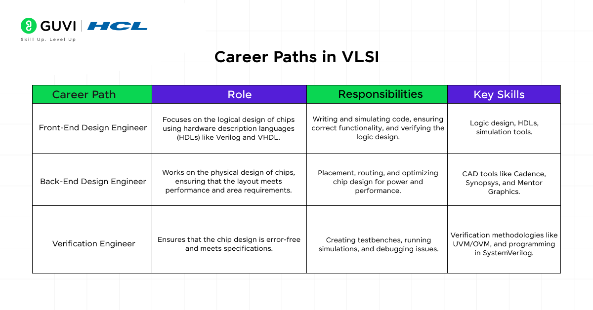
There are several pathways that a person pursuing VLSI can opt for. Here are some of the best career paths that are out there if you want to pursue a career in VLSI design.
1. Front-End Design Engineer
- Role: Focuses on the logical design of chips using hardware description languages (HDLs) like Verilog and VHDL.
- Responsibilities: Writing and simulating code, ensuring correct functionality, and verifying the logic design.
- Key Skills: Logic design, HDLs, simulation tools.
2. Back-End Design Engineer
- Role: Works on the physical design of chips, ensuring that the layout meets performance and area requirements.
- Responsibilities: Placement, routing, and optimizing chip design for power and performance.
- Key Skills: CAD tools like Cadence, Synopsys, and Mentor Graphics.
3. Verification Engineer
- Role: Ensures that the chip design is error-free and meets specifications.
- Responsibilities: Creating testbenches, running simulations, and debugging issues.
- Key Skills: Verification methodologies like UVM/OVM, and programming in SystemVerilog.
4. Analog Design Engineer
- Role: Designs analog circuits like amplifiers, oscillators, and power management units.
- Responsibilities: Developing high-performance analog components and integrating them with digital systems.
- Key Skills: Circuit design, SPICE simulation.
5. FPGA Design Engineer
- Role: Specializes in designing and implementing circuits on Field Programmable Gate Arrays (FPGAs).
- Responsibilities: Developing and testing FPGA-based solutions for applications like prototyping and custom hardware.
- Key Skills: FPGA programming, VHDL/Verilog, and debugging.
6. Embedded Systems Engineer
- Role: Combines VLSI knowledge with software to design embedded systems for specific applications.
- Responsibilities: Designing system-level solutions and ensuring seamless hardware-software integration.
- Key Skills: Embedded C, RTOS, and hardware-software co-design.
7. Semiconductor Process Engineer
- Role: Works in chip fabrication, focusing on the processes involved in manufacturing integrated circuits.
- Responsibilities: Optimizing fabrication techniques and ensuring high-quality production.
- Key Skills: Knowledge of semiconductor physics and fabrication processes.
Salary of VLSI Designers in India
Salaries for VLSI designers in India vary based on factors like experience, location, and the specific employer. Here’s an overview:
- Entry-Level Positions: Fresh graduates can expect starting salaries ranging from ₹1.8 lakh to ₹5 lakh per annum.
Collegedunia - Mid-Level Positions (2–5 years of experience): Professionals in this bracket typically earn between ₹5 lakh and ₹13 lakh per annum.
Collegedunia - Senior Positions (5+ years of experience): Experienced VLSI designers can command salaries upwards of ₹20 lakh per annum, with some earning as high as ₹37 lakh per annum. AmbitionBox
It’s important to note that these figures are approximate and can vary based on individual qualifications, negotiation, and company policies.
Find Out: Why is VLSI Used? A Comprehensive Exploration
VLSI Job Roles, Salary, Skills & Hiring Companies at a Glance
| VLSI Job Role | Avg Salary | Required Skills | Top Hiring Companies |
|---|---|---|---|
| Front-End Design Engineer | ₹4 lakh to ₹15 lakh per annum | Verilog, VHDL, digital logic design, simulation tools | Intel, Qualcomm, NVIDIA, Cadence Design Systems |
| Back-End (Physical) Design Engineer | ₹5 lakh to ₹18 lakh per annum | Cadence, Synopsys, Mentor Graphics, placement and routing | Synopsys, Cadence, Texas Instruments, Wipro |
| Verification Engineer | ₹5 lakh to ₹20 lakh per annum | UVM/OVM, SystemVerilog, testbench design | Qualcomm, AMD, HCL Technologies, Tessolve |
| Analog Design Engineer | ₹6 lakh to ₹20 lakh per annum | Circuit design, SPICE simulation, mixed-signal design | Texas Instruments, NXP, Analog Devices |
| FPGA Design Engineer | ₹4 lakh to ₹14 lakh per annum | FPGA programming, VHDL/Verilog, debugging | ARM, MediaTek, Samsung Semiconductor |
| Embedded Systems Engineer | ₹3.5 lakh to ₹12 lakh per annum | Embedded C, RTOS, hardware-software co-design | Wipro, HCL Technologies, Bosch |
| Semiconductor Process Engineer | ₹4 lakh to ₹16 lakh per annum | Semiconductor physics, fabrication processes | Intel, Micron, Tata Electronics |
Salary ranges are approximate and vary with experience, location, and company; treat them as directional rather than fixed figures. Figures are cross-checked against Glassdoor and AmbitionBox salary reports.
Is VLSI a Good Career in 2026?
Short answer: yes, and the job-openings data backs it up. Here’s what the numbers look like heading into 2026:
- Semiconductor hiring at India’s Global Capability Centers hit a peak in early 2026, with recruiter data pointing to over 3,500 open roles by March, according to a Careernet industry report.
- India currently hosts around 79 semiconductor design companies across roughly 180 units, already employing over 1.1 lakh professionals, and that base keeps expanding.
- Broader semiconductor hiring projections put the total number of new semiconductor jobs in India at around 10 lakh by FY2026–27, spanning fabrication, ATMP, chip design, VLSI, and embedded roles.
- Industry estimates suggest India will need an additional 85,000 to 100,000 VLSI engineers by 2030 to keep pace with new fabs and design centers.
Put together, this points to a genuine, structural shortage of skilled VLSI professionals rather than a short-term hiring spike, driven by India’s semiconductor mission, new fabrication plants, and global companies expanding their India design centers. The catch is that the gap isn’t in the number of engineering graduates; it’s in how many of them are industry-ready with practical skills in HDLs, CAD tools, and verification methodologies. That’s exactly why structured, hands-on VLSI training matters more than a theoretical degree alone.
Required Skills for a Career in VLSI
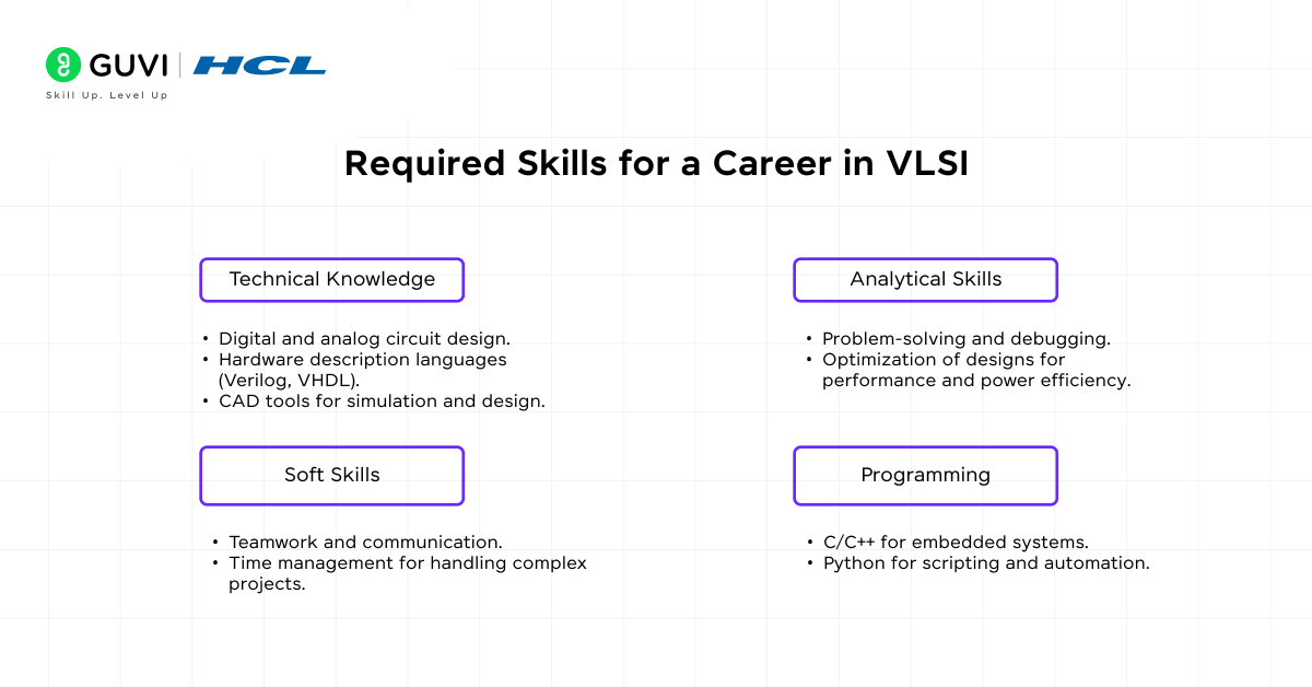
To build a successful career in VLSI, focus on developing the following skills:
- Technical Knowledge:
- Digital and analog circuit design.
- Hardware description languages (Verilog, VHDL).
- CAD tools for simulation and design.
- Analytical Skills:
- Problem-solving and debugging.
- Optimization of designs for performance and power efficiency.
- Programming:
- Soft Skills:
- Teamwork and communication.
- Time management for handling complex projects.
Getting Started with VLSI Design
If you’re intrigued by VLSI and want to dive deeper, here’s how you can get started:
- Learn the Basics of Electronics: Start with foundational topics like digital circuits, transistors, and logic gates.
- Explore Hardware Description Languages (HDLs): Tools like Verilog and VHDL are essential for designing chips.
- Use Design Tools: Get familiar with CAD tools like Cadence, Synopsys, or Mentor Graphics used for VLSI design.
- Study Fabrication Processes: Understanding how chips are manufactured can give you a broader perspective.
- Work on Projects: Build small-scale projects to apply what you learn and gain hands-on experience.
If you want to learn VLSI design through a step-by-step process guided by a professional mentor that includes Digital Electronics, UNIX, and even Shell Scripting, consider enrolling in HCL GUVI’s Certified VLSI Design Course which not only teaches you everything about the subject but also provides you with an industry-grade certificate!
Conclusion
In conclusion, VLSI design is an exciting field that blends creativity, problem-solving, and cutting-edge technology.
VLSI design is at the heart of the technological revolution, enabling the creation of smaller, faster, and smarter devices that define modern life.
As the demand for efficient and compact electronic systems continues to soar, the scope of VLSI design is set to expand further, making it an exciting time to explore this field.
FAQs
What is VLSI Design?
VLSI (Very Large Scale Integration) design involves integrating millions of transistors onto a single chip to create complex integrated circuits, forming the backbone of modern electronic devices.
What is the scope of VLSI in India?
India’s VLSI industry is expanding rapidly, with applications in consumer electronics, automotive, telecommunications, and healthcare, offering numerous career opportunities for skilled professionals.
What is the average salary of a VLSI Design Engineer in India?
Salaries vary based on experience and location; entry-level engineers earn between ₹1.8 lakh to ₹5 lakh per annum, while experienced professionals can earn up to ₹37 lakh per annum.
Which companies in India hire VLSI professionals?
Leading companies like Wipro, HCL Technologies, Qualcomm, Intel, and Cadence Design Systems actively recruit VLSI engineers in India.
What skills are essential for a career in VLSI design?
Key skills include a strong foundation in digital electronics, proficiency in hardware description languages like Verilog or VHDL, and experience with CAD tools used for chip design.
Success Stories

About the Author
Jebasta
I translate the language of data into stories that anyone can understand. As a writer with a data science background, I simplify analytics, AI, and decision-making so beginners and enthusiasts can confidently explore the world of data.
View all posts by Jebasta
Connect with me @

Did you enjoy this article?
Comments








It was really helpful for me to get more information about VLSI. Thank you so much for this article