


VLSI Design Articles
Semiconductors Explained: A Complete Guide to Modern Technology(2026)
High-Paying Jobs for Diploma Students in Semiconductor Industry in India
HCL GUVI for VLSI Training: Master Chip Design and Verification with Industry-Aligned Course
India's Semiconductor Mission: What It Means for ECE and Engineering Students in 2026–2027


Get In Touch For Details! Request More Information
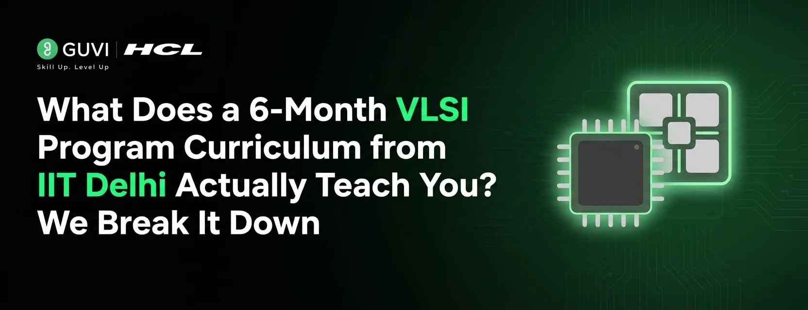
What Does a 6-Month VLSI Program Curriculum from IIT Delhi Actually Teach You? We Break It Down
May 04, 2026 7 Min Read 815 Views
(Last Updated)
TL;DR
- The VLSI Program Curriculum at Indian Institute of Technology Delhi covers the full RTL-to-GDSII chip design flow in 6 months
- Learn core areas: digital design, RTL coding, verification, physical design, low power, and packaging
- Get hands-on with EDA tools and complete 5 industry-style projects
- Build job-ready skills: RTL coding, debugging, STA, and design trade-offs
- Opens roles like VLSI Design, Verification, Physical Design, DFT, and FPGA Engineer
- Designed for ECE/EEE/CS students, graduates, and professionals aiming for semiconductor careers
The semiconductor industry is booming. India alone is projected to grow its share of global semiconductor sales from 6.5% to 11.5% by 2030, and nearly 20% of the world’s chip design engineers are already based here.
Yet the talent gap is enormous; the sector is expected to need 1 million professionals by 2026. The engineers who possess real, hands-on expertise in VLSI design are not just employable; they are in high demand.
That’s precisely why the Certificate Programme in Digital VLSI Design offered by the Continuing Education Programme (CEP) at IIT Delhi, India’s #1 ranked institution in the QS World University Rankings: India 2026, is designed the way it is.
It doesn’t cover surface-level theory. It takes you all the way from understanding a MOSFET to taping out a full chip design. In this blog, we break down the curriculum module by module so you know exactly what you’re signing up for.
What Is a VLSI Programme?
A VLSI programme is a structured course that teaches you how to design, verify, and implement integrated circuits, from RTL code to final chip layout. It is offered as university electives, postgraduate tracks, or industry-focused certifications.
It is ideal for ECE/EEE students, engineering graduates, or professionals moving into semiconductor roles. Basic knowledge of digital electronics or programming helps, but is not always required.
After completion, you can pursue roles like RTL Design Engineer, Verification Engineer, Physical Design Engineer, DFT Engineer, or STA Engineer. These are high-demand roles with salaries often 30–40% higher than comparable software jobs
Explore: How to learn a VLSI Course from Scratch?
Table of contents
- Why the Curriculum Structure Matters
- Skills You Gain from a VLSI Programme
- Career Opportunities After a VLSI Course
- Module 1: Digital IC Design: Where It All Starts
- Module 2: Scripting for VLSI Professionals: The Language of EDA
- Module 3: Logic Synthesis & Static Timing Analysis (STA)
- Module 4: Design for Testability (DFT) & Reliability
- Module 5: Physical Design: The Backend Story
- Module 6: Low Power & Advanced Design Techniques
- Module 7: Mixed-Signal & AMS Design
- Module 8: Packaging in VLSI
- The Projects: Where Learning Becomes Expertise
- Who Should Enrol?
- Final Thoughts
- Frequently Asked Questions
- What is this programme, and who offers it?
- Is this an IIT Delhi certificate? Will it say "IIT Delhi" on it?
- What does the curriculum cover?
- Is this a frontend or backend VLSI course?
- Who is eligible to apply?
- Do I need prior VLSI experience to join?
- How does the admission process work?
- How many seats are available?
- Is this programme fully online? Do I need to attend in person?
- What if I miss a live session?
- What kinds of jobs can I get after this programme?
- Who teaches this programme?
- How do I apply?
- What certificate will I receive?
Why the Curriculum Structure Matters
Before diving into the content, it helps to understand the philosophy behind this programme. VLSI design in industry has two broad domains: frontend (RTL design, synthesis, verification, timing) and backend (physical design, layout, DRC/LVS). Most courses cover one or the other.
This 6-month programme covers both, along with mixed-signal design, low-power techniques, packaging, and real hands-on projects. The result is a complete RTL-to-GDSII design engineer, exactly the profile that chipmakers at companies like Intel, Qualcomm, and Texas Instruments actively recruit for.
Read: How to Start a Career in VLSI in 2026: The Complete Roadmap
Core Components of a VLSI Program Curriculum
1. Basics of Electronics & Semiconductor Physics
Learn how semiconductors work, including PN junctions and MOSFETs, the foundation of all chip design.
2. Digital Design Fundamentals
Understand logic gates, combinational and sequential circuits, and FSMs to design digital systems.
3. HDL Programming
Write and simulate hardware using Verilog/VHDL and learn RTL coding for synthesis-ready designs.
4. RTL Design & Verification
Build efficient RTL and verify functionality using testbenches, simulation, and debugging techniques.
5. CMOS & Analog Basics
Explore CMOS logic, inverter design, and basic analog concepts for mixed-signal understanding.
6. Physical Design (Backend)
Convert designs into chip layouts through floorplanning, placement, routing, and verification.
7. VLSI Design Flow
Understand the complete RTL-to-GDSII flow from specification to chip tape-out.
8. EDA Tools & Hands-on Training
Gain practical experience with industry tools from Cadence Design Systems, Synopsys, and Siemens EDA.
9. Low Power & Advanced Topics
Learn power optimization, STA, DFT, and advanced techniques used in modern chip design.

Skills You Gain from a VLSI Programme
- RTL Coding: Write synthesisable Verilog/VHDL for hardware design
- Design Thinking: Balance timing, power, and area trade-offs
- Debugging & Verification: Identify and fix design issues efficiently
- EDA Tool Proficiency: Hands-on with tools from Cadence Design Systems, Synopsys, and Siemens EDA
Explore: VLSI Engineer Skills in 2026: What companies actually want.
Career Opportunities After a VLSI Course
- VLSI Design Engineer: RTL design and implementation
- Verification Engineer: Simulation and functional validation
- Physical Design Engineer: Backend design and chip layout
- FPGA Engineer: Prototype and optimize hardware systems
- DFT Engineer: Ensure chip testability and fault coverage
Explore: Top Companies Hiring for VLSI Professionals in 2026
Module 1: Digital IC Design: Where It All Starts
Every VLSI engineer, regardless of specialisation, must have a solid grounding in how CMOS circuits actually work. Module 1 addresses this foundational layer head-on.
You’ll study MOS device physics, how a MOSFET turns on and off, how it behaves at the transistor level, and then build upward to the CMOS inverter, the basic building block of all digital logic. From there, the module moves into combinational and sequential logic, including logic gates, flip-flops, and latches, all examined at the transistor level.
Critically, this module also introduces the CMOS ASIC design flow, giving you a bird’s-eye view of the entire chip design journey before you zoom into the details. This contextual awareness, knowing where each skill fits in the larger picture, is something that separates trained professionals from self-taught practitioners.
Break into the semiconductor industry with the skills companies actually hire for.
This programme by IIT Delhi, powered by HCL GUVI, takes you from RTL to GDSII with hands-on projects and real EDA workflows
Ready to design chips, not just study them?
Apply now to the Certificate Programme in Digital VLSI Design by Indian Institute of Technology Delhi, delivered with support from HCL GUVI, and start building real, industry-ready skills before applications close.
Module 2: Scripting for VLSI Professionals: The Language of EDA
Modern VLSI design doesn’t happen manually. Every major step, synthesis, place and route, timing analysis, and simulation is controlled through scripts. If you want to work efficiently in any EDA (Electronic Design Automation) environment, you need to be fluent in Linux, TCL, Perl, and Python.
Module 2 starts by building a proper Linux environment, then introduces each scripting language in the context of VLSI workflows. You’ll learn how to automate RTL coding, design flows, and verification tasks. The module also covers RTL coding and design styles, writing efficient, synthesisable HDL code that EDA tools can process reliably.
This might seem like a “soft” skill, but in practice, scripting proficiency directly determines how fast and effectively an engineer can work. Professionals who can write clean automation scripts are far more productive and far more valuable to a team
Module 3: Logic Synthesis & Static Timing Analysis (STA)
This is where frontend design gets serious. Logic synthesis is the process of translating your RTL code into an actual gate-level netlist, with real logic gates from a technology library. Module 3 covers synthesis concepts and optimisation strategies, including power-aware synthesis, which has become critical in modern low-power chip design.
The second half of this module focuses on Static Timing Analysis (STA): one of the most important skills in the entire VLSI domain. STA is how you verify that your chip will actually work at the target clock frequency. You’ll learn timing concepts like setup time, hold time, slack, and timing paths, and understand how to achieve timing closure. If you’ve ever wondered why chip design engineers spend so much time on timing, this module will make everything clear.
Module 4: Design for Testability (DFT) & Reliability
A chip that can’t be tested can’t be manufactured at scale. Module 4 addresses Design for Testability, a discipline that ensures your design can be efficiently verified after fabrication.
You’ll learn about fault models and fault coverage metrics, and how engineers quantify whether a test is thorough enough. The module then covers scan chain insertion and ATPG (Automatic Test Pattern Generation), which are the industry-standard techniques used to test digital ICs in mass production. BIST (Built-In Self-Test) techniques are also covered.
Beyond testability, this module also tackles reliability in nano-scale VLSI, soft errors, noise margins, and resilience challenges that arise when transistors shrink to a few nanometers. As devices get smaller, reliability becomes harder to guarantee, and engineers who understand these challenges are increasingly sought after.
Module 5: Physical Design: The Backend Story
Now we move to the backend: translating your gate-level netlist into a real, manufacturable chip layout. Module 5 covers the complete physical design flow:
- Floorplanning: Deciding where different functional blocks live on the chip
- Placement: Positioning individual cells within those blocks
- Clock Tree Synthesis (CTS): Building the clock distribution network to minimise skew
- Power Planning: Ensuring adequate power delivery across the chip
- Routing: Connecting everything with metal wires
The module also addresses advanced node challenges such as FinFET transistor architectures, EUV lithography, and double patterning, the technologies that make modern chips at 7nm, 5nm, and below possible. Understanding these challenges is essential for anyone aiming at cutting-edge semiconductor work.
Module 6: Low Power & Advanced Design Techniques
Power consumption is one of the biggest challenges in modern chip design. A chip that runs too hot or drains a battery too quickly is commercially unviable regardless of how functionally correct it is. Module 6 is entirely dedicated to solving this problem.
You’ll learn the sources of power dissipation in CMOS circuits, dynamic power, static leakage, and short-circuit power, and then master the methodologies to address each: clock gating, multi-threshold voltage (multi-Vt) design, multi-voltage domains, Dynamic Voltage and Frequency Scaling (DVFS), and power gating. You’ll also work with UPF/CPF (Unified Power Format / Common Power Format) , the industry-standard specification languages for power-aware design, used by every major semiconductor company today.
Module 7: Mixed-Signal & AMS Design
The real world isn’t purely digital. Every chip that communicates with sensors, displays, or wireless networks has analog components. Module 7 introduces mixed-signal and Analog-Mixed Signal (AMS) design, the integration of analog and digital blocks on the same chip.
You’ll cover the basics of analog IC design, including amplifiers and reference circuits, before moving to the challenges of mixed-signal integration: managing noise coupling, signal integrity, and layout constraints when analog and digital circuits share silicon. The module also covers Phase-Locked Loops (PLLs) and clock generation circuits, ubiquitous components in any communication or high-speed digital chip.
Module 8: Packaging in VLSI
A chip without a package is a chip that can’t be used. Module 8 rounds out the curriculum by covering IC packaging technologies, from traditional wire bonding to advanced flip-chip and system-in-package (SiP) techniques. You’ll study the electrical, thermal, and mechanical considerations that affect chip performance after it leaves the fab.
With the global push toward chiplets and heterogeneous integration, packaging knowledge has become a distinct competitive advantage for VLSI engineers.
The Projects: Where Learning Becomes Expertise
Theory alone doesn’t build engineers. The programme includes five hands-on projects that put every module to work:
- Combinational and Sequential CMOS Circuit Design: transistor-level design with functional verification
- Low Power I/O Circuit Design: designing input buffers, output drivers, and level shifters
- Power Management IC (PMIC) Design: voltage regulators and power delivery circuits
- Clock Tree Synthesis and STA: end-to-end timing analysis and closure
- DFT and ATPG: scan insertion and test pattern generation for high fault coverage
These aren’t toy exercises. They’re structured to mirror real industry workflows, building the EDA tool proficiency and problem-solving confidence that employers look for.
Looking for the most practical way to break into chip design?
HCL GUVI for VLSI Training brings you the Certificate Programme in Digital VLSI Design by Indian Institute of Technology Delhi, a complete RTL to GDSII learning experience built for real industry roles.
With expert-led sessions, hands-on projects, and end-to-end curriculum delivery powered by HCL GUVI, this is where your VLSI career starts.
Who Should Enrol?
The programme is open to graduates in Electronics, Electrical Engineering, Physics, or Computer Science, as well as diploma holders and final-year students. Admission considers academic background, work experience, and an interview.
With VLSI design engineers commanding up to 40% higher starting pay than typical software roles, and career trajectories moving from Design Engineer to Chip Architect within 7–8 years, the return on this investment is substantial.
Final Thoughts
The VLSI curriculum at CEP, IIT Delhi, isn’t designed to give you a certificate to display on your wall. It’s designed to make you someone the semiconductor industry actually needs, a professional who understands both the physics of transistors and the practicalities of taping out a chip. In a sector growing at 9.2% CAGR globally and adding millions of jobs in India alone, that expertise is one of the most valuable things you can invest in.
If you are serious about building a career in chip design, the right training matters. HCL GUVI VLSI Training offers the Certificate Programme in Digital VLSI Design by Indian Institute of Technology Delhi, giving you a complete RTL to GDSII learning experience aligned with real industry workflows.
With expert-led sessions, practical projects, and structured guidance delivered by HCL GUVI, you are not just learning concepts; you are building the skills companies hire for.
Frequently Asked Questions
1. What is this programme, and who offers it?
This is a 6-month Certificate Programme in Digital VLSI Design offered by the Continuing Education Programme (CEP) at IIT Delhi. India’s #1-ranked institution in QS World University Rankings: India 2026 and #2 in NIRF 2025 under the Engineering category. It is a live online programme designed to train electronics and CS graduates in end-to-end chip design, from RTL coding all the way to physical layout and verification.
2. Is this an IIT Delhi certificate? Will it say “IIT Delhi” on it?
Yes. Certificates are issued directly by the Continuing Education Programme (CEP), IIT Delhi. Candidates who meet the completion criteria receive a Certificate of Completion from CEP, IIT Delhi. Certificates are issued as e-certificates only.
3. What does the curriculum cover?
Digital IC Design (CMOS fundamentals, MOS device physics)
Scripting for VLSI Professionals (Linux, TCL, Perl, Python)
Logic Synthesis & Static Timing Analysis (STA)
Design for Testability (DFT) & Reliability
Physical Design (Floorplanning, Placement, CTS, Routing)
Low Power & Advanced Design Techniques
Mixed-Signal & AMS Design
IC Packaging
Plus 5 hands-on projects and an optional 3-day campus immersion at IIT Delhi.
4. Is this a frontend or backend VLSI course?
Both. The programme covers the complete RTL-to-GDSII design flow , frontend (RTL design, synthesis, timing analysis, DFT) as well as backend (physical design, clock tree synthesis, routing, power planning). This makes it one of the most comprehensive VLSI programmes available in an online format.
5. Who is eligible to apply?
The programme is open to:
Graduates in Electronics, Electrical Engineering, Physics, or Computer Science
Candidates currently pursuing a graduation degree (preference given to those with work experience)
Diploma holders (10+2+3 or 10+3 format) are also eligible
To Know More: Everything You need to about VLSI Course Eligibility
6. Do I need prior VLSI experience to join?
Prior VLSI experience is not mandatory, but a background in electronics or computer science is expected. The curriculum begins with device-level fundamentals before advancing to industry workflows. Candidates with some work experience are given preference during admission.
7. How does the admission process work?
Admission is based on three factors:
Academic background
Professional background/work experience
Performance in the interview process
The Programme Coordinator(s) at IIT Delhi shortlist and select candidates. Screening and final selection are conducted by the IIT Delhi Programme Coordinator.
8. How many seats are available?
The brochure does not specify a fixed seat count, but as admission is selective and based on an interview process, early application is strongly recommended.
9. Is this programme fully online? Do I need to attend in person?
The programme is delivered as Live Online sessions.
There is an optional 3-day campus immersion at IIT Delhi, which, while not mandatory, is highly recommended for in-person faculty interaction, peer networking, and hands-on reinforcement of concepts. Travel and accommodation for the campus visit are at the participant’s expense.
10. What if I miss a live session?
A minimum of 50% attendance is required to be eligible for the certificate. It is advisable to attend live sessions as much as possible and clarify the recording policy directly with the programme team before enrolling.
11. What kinds of jobs can I get after this programme?
The programme prepares you for roles such as:
VLSI Design Engineer
RTL Design Engineer
Physical Design Engineer
DFT Engineer
Static Timing Analysis (STA) Engineer
Low Power Design Engineer
Mixed-Signal Design Engineer
Chip Architect (with experience)
VLSI design engineers typically earn up to 40% more than equivalent software roles at the same career stage.
12. Who teaches this programme?
The programme is coordinated and taught by faculty from IIT Delhi’s Centre for Applied Research in Electronics (CARE):
13. How do I apply?
Applications are submitted online. Visit https://cepqip.iitd.ac.in/ for the application link and further details.
14. What certificate will I receive?
You can earn either a Certificate of Participation (50% attendance) or a Certificate of Completion (50% attendance + 60% marks), both issued as e-certificates by IIT Delhi Continuing Education Programme.
Success Stories

About the Author
Salini Balasubramaniam
A curious, information-savvy writer loves to turn deep insights into authentic and engaging content that connects. With experience in writing for brands and driving audience engagement, I believe that words can make a powerful difference.
View all posts by Salini Balasubramaniam
Connect with me @


Did you enjoy this article?