

VLSI Design Articles
What is Low Power VLSI Design? A Beginner’s Guide to Power Optimization
The Role of VLSI in Electric Vehicles: How Chip Design Powers India's EV Revolution
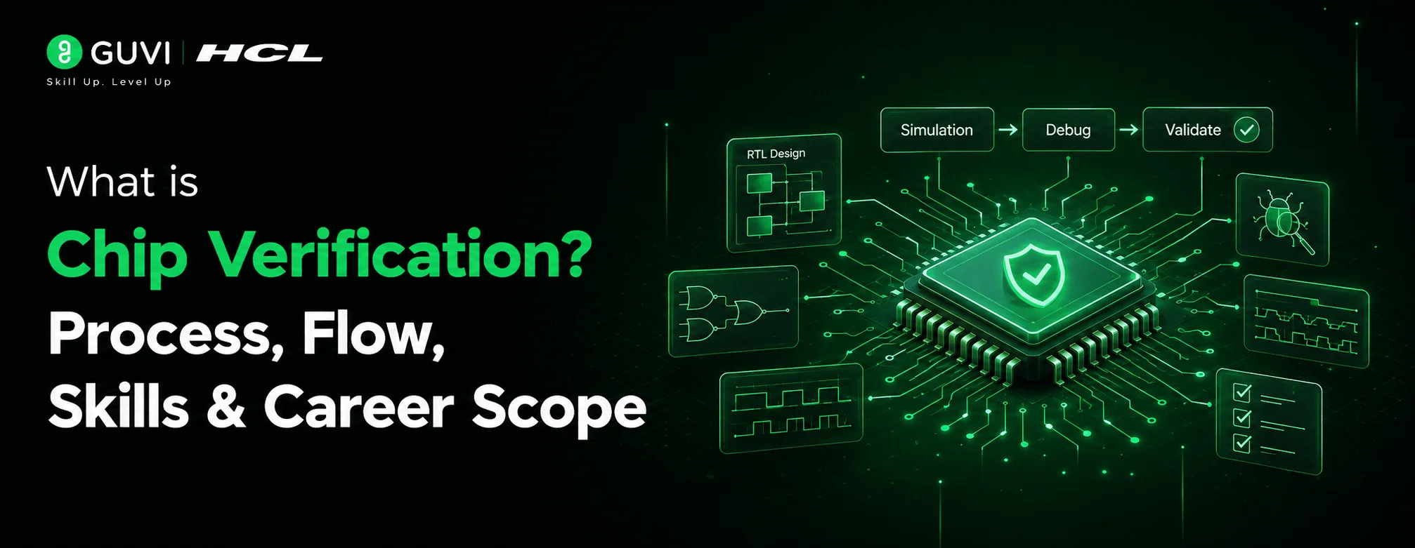
What is Chip Verification? Process, Flow, Skills & Career Scope

Get In Touch For Details! Request More Information

How to Start a Career in VLSI in 2026: The Complete Roadmap
Jul 20, 2026 9 Min Read 2016 Views
(Last Updated)
With AI-driven technologies reshaping the semiconductor industry in 2026, the demand for VLSI engineers is growing faster than ever.
According to industry reports, the global semiconductor market is projected to exceed $1 trillion by 2030, highlighting the massive need for skilled professionals in chip design and development.
Many beginners struggle to understand how to start a career in VLSI, what skills are actually required, and which domain to choose in such a vast field.
At the same time, trends such as AI accelerators, electric vehicles, and IoT devices are rapidly increasing demand for specialized chips, making VLSI a critical and future-proof career path.
If you are searching for a clear roadmap to enter this field, this guide addresses exactly that. It breaks down the VLSI ecosystem, required skills, and career paths, helping students, graduates, and career switchers understand how to start a career in VLSI in 2026 with clarity and confidence.
Three major forces are reshaping the semiconductor industry:
- AI Revolution: Driving demand for GPUs, NPUs, and TPUs at massive scale
- Electric Vehicles (EVs): Increasing need for power electronics and embedded chips
- IoT Expansion: Creating demand for low-power, highly integrated SoCs
Table of contents
- TL;DR Summary
- India’s Semiconductor Opportunity
- Major Investments Already Underway
- Why VLSI is a Great Career Choice in 2026
- How the VLSI Ecosystem Works
- Prerequisites and Educational Background for VLSI and Embedded Systems
- Do you need a Master's degree?
- The VLSI Domain Roadmap: Pick Your Lane
- B. Functional Verification
- C. Physical Design (PD)
- d. DFT (Design for Testability)
- E. Analog and Mixed-Signal Design
- Must-Have Skills in 2026
- Learning Resources and Certifications
- Building Your Portfolio
- Internships and First Job Strategy
- Top Companies Hiring VLSI Freshers in India (2026):
- Salary Expectations and Career Growth
- Conclusion
- Frequently Asked Question
- What is VLSI Design, and why is it important in 2026?
- How can a beginner start a career in VLSI?
- Is VLSI a good career option in India in 2026?
- Do I need a Master’s degree to get a VLSI job?
- Which VLSI domain is best for freshers?
- What programming languages are required for VLSI?
- How long does it take to learn VLSI?
- What are the best tools to learn for VLSI beginners?
- What is the salary of a VLSI engineer in India?
- What projects should I build to get a VLSI job?
TL;DR Summary
- The semiconductor industry is booming, with the market expected to exceed $1 trillion by 2030, creating high demand for VLSI engineers.
- AI, electric vehicles, and IoT are the key drivers increasing the need for advanced chip design.
- Beginners often struggle due to unclear skill requirements and multiple domain choices.
- Start by understanding the VLSI ecosystem, then focus on one domain like RTL design, verification, or physical design.
- Build strong fundamentals in digital electronics and learn Verilog or SystemVerilog, along with Linux and scripting.
- Work on hands-on projects such as a RISC-V core or RTL-to-GDSII flow to stand out.
- Functional verification is the most in-demand and beginner-friendly entry point.
- With consistent effort over 6–12 months, you can become job-ready in this high-growth field.
India’s Semiconductor Opportunity
India is at a pivotal moment in its semiconductor journey, and the timing has never been better for engineers looking to build a career in VLSI domestically.
The Indian government has committed significant funding to building domestic semiconductor manufacturing infrastructure. This policy-level commitment is translating into real facilities and real jobs on the ground.
Major Investments Already Underway
- Tata’s partnership with PSMC to build a semiconductor fabrication plant in Gujarat
- Micron’s assembly and testing facility in Sanand, marking one of the biggest foreign semiconductor investments in India’s history
These are not announcements; they are active projects that signal a major structural shift in where chips are designed, assembled, and tested.
- Growing Local Hiring. Top global companies like Texas Instruments, Qualcomm, Intel, and MediaTek already have significant engineering centres in Bengaluru and Hyderabad.
Alongside them, homegrown startups like InCore
- Semiconductors, Mindgrove Technologies, and Saankhya Labs are growing rapidly, offering faster learning curves and exciting early-stage opportunities.
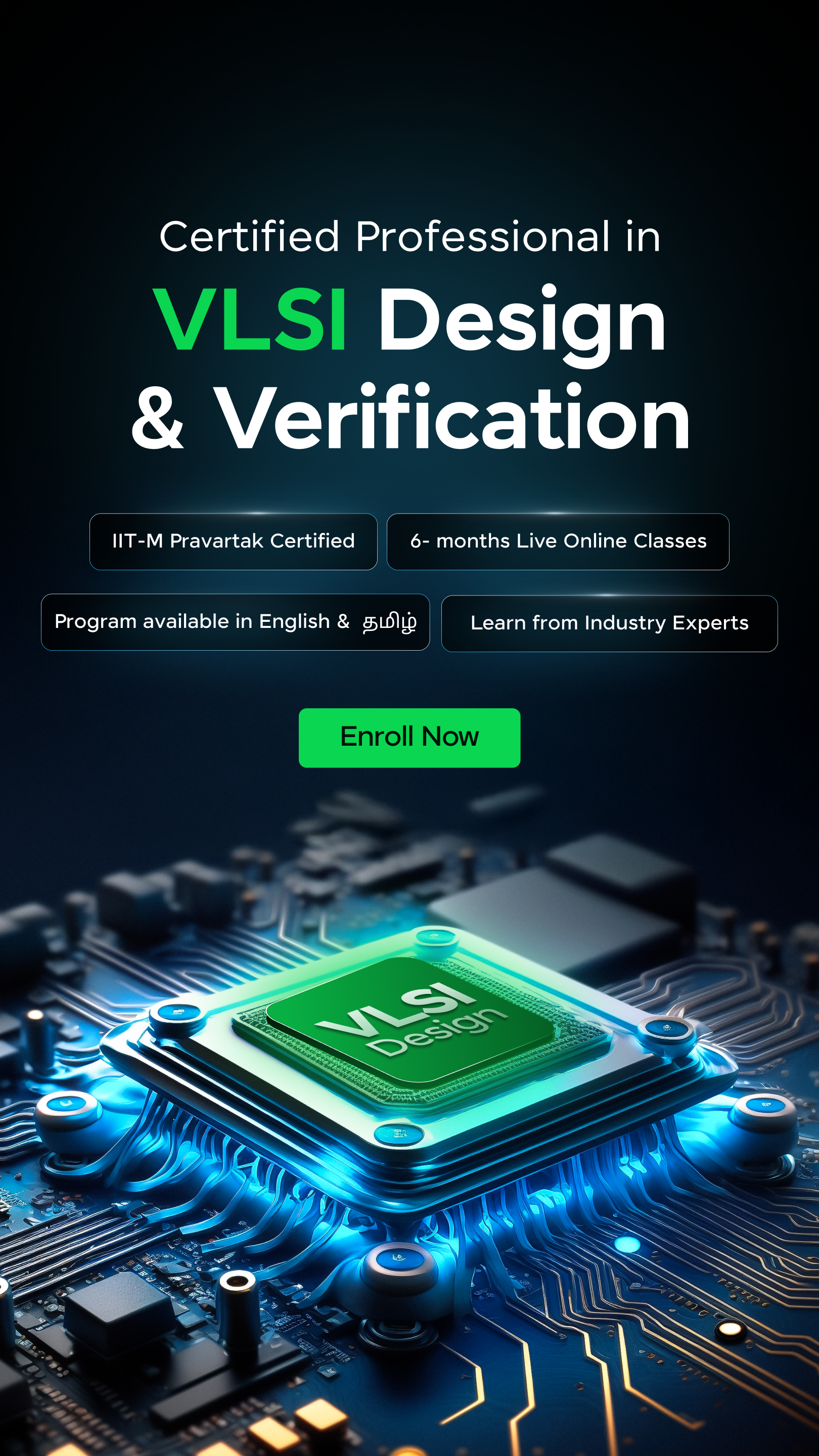
If you want to build a strong foundation in VLSI design through a structured, step-by-step approach that covers digital electronics, circuit design, and real-world applications, consider enrolling in HCL GUVI’s Certified VLSI Course, which not only equips you with industry-relevant skills but also provides a recognized certification to boost your career.
1. Why VLSI is a Great Career Choice in 2026
The world fundamentally runs on chips, and every smartphone, electric vehicle, AI model, and IoT device traces back to silicon, with advanced integrated circuits built on a single chip powering smarter connected products.
VLSI is the field that makes all of it possible, and right now, demand for skilled engineers is not just growing, it’s surging.
Three major forces are driving this:
AI Revolution: The explosion of artificial intelligence has created massive demand for specialized processors like GPUs, NPUs, and TPUs, making chip development a long-term growth area and increasing demand for high performance computing hardware.
Electric Vehicles: The EV industry’s rapid growth has increased the need for power electronics and embedded chips significantly, and similar design skills are also used in medical devices and defense systems.
IoT Expansion: Billions of connected devices need low-power, highly integrated SoCs, creating a steady and growing pipeline of chip design work, especially for reliable communication systems.
On top of these global trends, India specifically presents a unique opportunity.
With the India Semiconductor Mission, government funding, and global companies like Tata, Micron, and TSMC expanding their presence in the country, local career opportunities are multiplying fast, with demand rising for vlsi professionals across consumer electronics and other sectors.
For engineers willing to invest in the right skills, VLSI offers not just strong salaries but the satisfaction of knowing your work powers technology used by millions of people worldwide.

2. How the VLSI Ecosystem Works
Before you start learning tools and languages, you need to understand how chips are actually built.
The semiconductor design and manufacturing process is called the chip design flow. It runs roughly like this:
RTL Design > Functional Verification > Synthesis > Physical Design > Fabrication > Testing
At the RTL (Register Transfer Level) stage, engineers write the chip’s behaviour in hardware description languages like Verilog or VHDL.
This is the “what does this chip do?” stage. Verification engineers then run the design through thousands of simulation tests to make sure it works correctly.
Once verified, synthesis tools convert the RTL into a gate-level netlist, which is a network of logic gates.
Physical Design engineers then figure out how to arrange and connect billions of transistors on a silicon chip.
Fabrication, done by foundries like TSMC or Samsung, turns that layout into real silicon.
Finally, testing engineers check that manufactured chips meet specifications before they ship.
The industry is broadly split into two areas:
Frontend covers RTL Design and Functional Verification.
You work with logic, behaviour, and simulation. It is closer to software in some ways, but still rooted in digital logic.
Backend covers Physical Design, DFT (Design for Testability), Timing Analysis, and Analog/Mixed-Signal Design.
A quick look at the VLSI industry landscape
You work with layout geometry, power, and manufacturing constraints.
The major players span several categories. On the design and manufacturing side, you have Intel, TSMC, Qualcomm, Samsung, NVIDIA, AMD, Arm, Apple, and MediaTek.
On the tools and IP side, Synopsys, Cadence, and Siemens EDA (Mentor) lead the market.
Knowing what each of these companies does will help you target your job search smartly.
If you aim to kickstart your career in chip design with a comprehensive program covering digital systems, practical labs, and real-world scenarios, then HCL GUVI VLSI course is a great choice to develop job-ready skills along with a valuable certification.
3. Prerequisites and Educational Background for VLSI and Embedded Systems
Most VLSI roles require a strong base in electrical engineering. The most common entry paths are:
- B.E./B.Tech in ECE (Electronics and Communication Engineering), which is the most common background
- B.E./B.Tech in EEE (Electrical and Electronics Engineering)
- Computer Engineering, especially for frontend roles
- Applied Physics or Nanotechnology, for device engineering and process roles
No matter your degree, these are the subjects that matter most:
- Digital Electronics is the backbone of RTL and verification work
- Semiconductor Physics and Devices is important for analog, physical design, and device engineering
- Computer Architecture is essential for design, verification, and understanding SoC behaviour
- Signals and Systems is foundational for analog and mixed-signal roles
- VLSI Design should be taken seriously if it is in your curriculum; if not, study it on your own
4. Do you need a Master’s degree?
This is one of the most common questions, and the honest answer is: it depends.
In India, many top companies like Texas Instruments, Qualcomm, and Intel hire B.Tech graduates directly. This is especially true for verification and physical design roles, as long as you have strong fundamentals, good projects, and some tool experience.
However, for research roles, analog design positions, or roles at companies like Apple and NVIDIA, a Master’s degree from a good institution gives you a real advantage.
If you are targeting a career in the US, Europe, or Singapore, an M.S. from a recognised university is almost required for full-time roles at top companies.
If you are staying in India and are focused, a strong skill-building plan can get you there without a Master’s degree, but it takes discipline and a solid portfolio.
4. The VLSI Domain Roadmap: Pick Your Lane
VLSI is not one career. It is a family of careers. The biggest mistake beginners make is trying to learn everything at once.
Instead, pick one area early, go deep, and expand from there. Here is a breakdown of the major domains:
- RTL Design
RTL designers translate architecture specifications into synthesizable hardware description code. This is where a chip’s functionality comes to life.
What to learn:
- Hardware Description Languages: Start with Verilog, then move to SystemVerilog. VHDL is good to know, especially for defence and aerospace work
- Design concepts: FSMs, pipelines, arbiter design, clock domain crossing, reset strategies, and bus protocols like AXI, APB, and AHB
- Tools: Xilinx Vivado for FPGA-based simulation, and ModelSim or QuestaSim for industry-standard simulation
Career fit: RTL design is a good fit if you enjoy logic-level problem solving and are comfortable thinking in terms of state machines and timing diagrams.
Also Explore: What is VLSI Design? A complete Guide
B. Functional Verification
Verification engineers make sure a chip design is correct before fabrication begins. A chip tape-out can cost anywhere from one million to one hundred million dollars, depending on the process node. Bugs are not an option.
What to learn:
- SystemVerilog for writing testbenches
- UVM (Universal Verification Methodology), which is the industry-standard framework for structured verification
- Basic Formal Verification using tools like JasperGold or Questa Formal
- Coverage-driven verification, including functional coverage and code coverage
- Assertion-based verification using SVA (SystemVerilog Assertions)
Why it matters in 2026: Functional verification is widely considered the most in-demand VLSI role in the world right now.
Modern SoCs have billions of transistors, dozens of IP blocks, and multiple clock domains. Verification teams are often larger than design teams. If you want the fastest path to employment in VLSI, verification is it.
C. Physical Design (PD)
Physical Design engineers take a verified, synthesised netlist and plan how to physically build it on silicon. They must meet timing, power, area, and design rule requirements.
What to learn:
- Core concepts: Floorplanning, Power Planning, Placement, Clock Tree Synthesis (CTS), Routing, and Sign-off
- Static Timing Analysis (STA): Understanding setup and hold violations, timing paths, and constraints
- Tools: Cadence Innovus for place and route, Synopsys ICC2, and PrimeTime for STA sign-off
- Scripting: Tcl is required for this role since physical design work is heavily scripted
Career fit: Physical Design suits engineers who enjoy working at the intersection of circuit physics and practical problem-solving. Comfort with Linux and scripting is important. Senior PD engineers are among the highest-paid professionals in the VLSI field.
d. DFT (Design for Testability)
DFT engineers make sure a manufactured chip can be tested effectively after fabrication. Without DFT, there is no reliable way to confirm a chip works correctly once it comes off the production line.
What to learn:
- Scan insertion and scan chain architecture
- ATPG (Automatic Test Pattern Generation)
- BIST (Built-In Self-Test) for memory and logic
- Boundary Scan and JTAG
- Tools: Synopsys TetraMAX and Mentor Tessent
Why it matters: As chips grow more complex, DFT is becoming more sophisticated and more critical. It is a niche that many engineering programmes do not cover well, which makes it a strong entry point with less competition than RTL or verification roles.
E. Analog and Mixed-Signal Design
Analog design deals with circuits that work in the continuous domain, including amplifiers, oscillators, filters, PLLs, ADCs, and DACs. Mixed-signal design sits at the boundary between analog and digital.
What to learn:
- Core circuits: Op-amps, bandgap references, PLLs, LDOs, ADCs, and DACs
- CMOS circuit design theory at the transistor level
- Tools: Cadence Virtuoso for design and Spectre for simulation
- Layout: DRC, LVS, and parasitics
Reality check: Analog design has one of the highest skill ceilings in VLSI and one of the steepest learning curves. It is not a good starting point unless you have a strong academic foundation in analog circuits. That said, if you are passionate about it, the career ceiling is very high, and the pool of qualified engineers is small.
The global semiconductor industry is projected to exceed $1 trillion by 2030.
India’s semiconductor mission includes multi-billion-dollar investments from companies like Tata Group and Micron.
The semiconductor workforce demand is growing rapidly due to the expansion of AI, EVs, and IoT.
5. Must-Have Skills in 2026
Technical knowledge in your domain is necessary, but not enough on its own. Here are the cross-domain skills that will separate you from other candidates:
Scripting and Automation: Modern VLSI flows are heavily automated. Python is important for data analysis, flow automation, and reporting. Tcl is required for working with EDA tools from Cadence and Synopsys. Perl is still used in many legacy flows. If you cannot write scripts, you will hit a ceiling quickly.
Version Control with Git: Chip design projects involve large codebases with many contributors. Learn how to use Git, including branching, merging, and pull requests. It seems basic, but many VLSI freshers skip it and regret it later.
Linux Command Line: Almost every professional EDA tool runs on Linux. If you are not comfortable with a Linux terminal, managing file permissions, writing shell scripts, or running jobs on a compute cluster, start practising now.
6. Learning Resources and Certifications
You do not need an expensive degree programme to learn VLSI. Here is a curated list of resources that actually work:
Free Resources:
- NPTEL courses like “Hardware Modeling Using Verilog” are structured, credible, and completely free
- Nandland on YouTube and its website is one of the best free resources for FPGA and Verilog learning
- VLSIGuru on YouTube is good for physical design concepts
- GitHub has many open-source RTL projects, RISC-V cores, and UVM testbench examples worth studying.
- Tiny Tapeout lets you get a simple design manufactured on real silicon as part of a community project
Paid Courses and Platforms:
- VSD (VLSI System Design) is one of the most respected platforms for practical VLSI learning in India. It covers physical design, RTL, and the full chip flow
- HCL GUVI is a self-paced course help you to build a strong foundation in Very Large Scale Integration (VLSI) with a comprehensive digital electronics program.
- Maven Silicon offers structured training programmes with placement support
- Udemy has good SystemVerilog, UVM, and FPGA courses. Look for ones with strong reviews
Certifications:
- Cadence Skill Certification carries real weight in the industry, especially for PD and analog roles
- Synopsys Training Programs are recognised by HR teams at companies that use Synopsys tools
The most important thing to remember: do not just watch courses. Build things.
7. Building Your Portfolio
In VLSI, your GitHub profile and project portfolio matter just as much as your resume. Here is what a strong portfolio looks like:
Design a basic processor. Implement a simple RISC-V core in SystemVerilog. Even a 5-stage pipelined RV32I design shows that you understand computer architecture, HDL coding, and simulation. Document it clearly.
Run an RTL-to-GDSII flow. Use OpenLane and the Sky130 PDK to take a small design from RTL all the way to a physical layout. A counter, a simple ALU, or a UART module works fine. Very few freshers do this, so it signals strong hands-on ability to recruiters.
Write a UVM testbench. Pick a standard interface like SPI or I2C and build a structured UVM environment around it. This means creating an agent, driver, monitor, scoreboard, and coverage model. Push the project to GitHub.
Contribute to open-source chip design. Projects like OpenROAD, the CHIPS Alliance, or ZipCPU are actively maintained. Even a small bug fix or a documentation update shows that you can work in a real collaborative engineering environment.
Document everything on GitHub and LinkedIn. Write a short LinkedIn post about each project. Engineers who can explain their work clearly stand out. VLSI is highly technical, but being able to describe what you built and why matters a lot in interviews
Explore: VLSI Interview Question and Answer for Professionals
8. Internships and First Job Strategy
Where to Find VLSI Internships:
- LinkedIn: Set up job alerts for “VLSI intern,” “RTL design intern,” “physical design intern,” and “verification intern.”
- Internshala: Used actively by Indian semiconductor startups and mid-sized companies
- Company portals: Texas Instruments, Intel, Qualcomm, and MediaTek all run structured internship programmes. Apply directly through their websites
- College placement cells: If you are a student, use this channel aggressively. Many companies visit campuses only through formal placement tie-ups
Top Companies Hiring VLSI Freshers in India (2026):
- Texas Instruments India (Bengaluru): One of the biggest and most respected VLSI employers in India. Hires heavily for analog, verification, and embedded roles
- Qualcomm India: Strong in modem, RF, and AI chip design. Competitive, but highly rewarding
- Intel India (Bengaluru, Hyderabad): Hires broadly across physical design, verification, and DFT
- MediaTek India: Rapidly expanding with strong hiring in verification and RTL
- Wipro VLSI and HCL Technologies: Service-based VLSI work. A solid entry point for freshers building industry experience
- Semiconductor startups like InCore Semiconductors, Mindgrove Technologies, and Saankhya Labs: Smaller teams, faster learning, and growing funding
9. Salary Expectations and Career Growth
Here are realistic salary benchmarks for VLSI engineers in 2026:
| Experience Level | Average Salary in India |
| Fresher (0 to 1 year) | 5.8 LPA to 6.4 LPA |
| Mid-level (3 years) | 22 LPA to 27 LPA |
| Senior (5 years) | 24 LPA to 40 LPA |
| Lead or Architect (8 to 12 years) | 40L to 80L+ |
The typical VLSI career ladder looks like this:
Graduate Engineer > Engineer > Senior Engineer > Staff Engineer or Lead > Principal Engineer > Architect or Distinguished Engineer.
Switching between VLSI domains is possible, but it takes focused effort. Moving from verification to physical design, for example, means picking up STA, Tcl scripting, and PnR tools.
However, the logical thinking skills from verification transfer well. Many senior VLSI engineers have worked across two or three domains over their careers.
Conclusion
Starting a career in VLSI in 2026 is a smart and future-proof choice. The path is challenging, but with the right fundamentals, a clear domain focus, and hands-on projects, you can build a strong entry into the industry.
With AI, EVs, and IoT driving massive chip demand, opportunities are only growing. Focus on real skills over theory, stay consistent, and build a solid portfolio.
VLSI isn’t easy, but the reward of seeing your work powering real-world technology makes it worth it.
Frequently Asked Question
1. What is VLSI Design, and why is it important in 2026?
VLSI (Very Large Scale Integration) is the process of designing and integrating millions or billions of transistors into a single chip. In 2026, it is critical because it powers technologies like AI chips, smartphones, electric vehicles, and IoT devices.
2. How can a beginner start a career in VLSI?
Start by building a strong foundation in digital electronics, then learn hardware description languages like Verilog or SystemVerilog. Choose a domain (RTL, verification, or physical design), work on projects, and build a portfolio on GitHub.
3. Is VLSI a good career option in India in 2026?
Yes, VLSI is one of the fastest-growing careers in India due to initiatives like the India Semiconductor Mission, increasing chip demand, and the expansion of global semiconductor companies in India.
4. Do I need a Master’s degree to get a VLSI job?
No, a Master’s degree is not mandatory. Many companies like Intel and Qualcomm hire B.Tech graduates. However, a Master’s helps for advanced roles, especially in analog design and research.
5. Which VLSI domain is best for freshers?
Functional verification is currently the most beginner-friendly and in-demand domain. It uses methodologies like UVM and offers faster entry into the industry compared to RTL or analog design.
6. What programming languages are required for VLSI?
Key languages include Verilog/SystemVerilog for design and verification, along with scripting languages like Python and Tcl. Knowledge of Linux is also essential for working with EDA tools.
7. How long does it take to learn VLSI?
With consistent effort, it typically takes 6–12 months to become job-ready in one domain. This includes learning concepts, tools, and completing hands-on projects.
8. What are the best tools to learn for VLSI beginners?
Some widely used tools include:
Cadence Innovus for physical design
ModelSim for simulation
OpenLane for end-to-end chip design
9. What is the salary of a VLSI engineer in India?
Freshers can earn between ₹4 LPA and ₹12 LPA, depending on skills and company. With experience, salaries can grow significantly, especially in high-demand domains like physical design and verification.
10. What projects should I build to get a VLSI job?
Strong beginner projects include:
Designing a RISC-V processor
Running an RTL-to-GDSII flow using OpenLane
Building a verification environment using UVM
These projects demonstrate practical skills and improve your chances of getting hired.
Success Stories

About the Author
Salini Balasubramaniam
A curious, information-savvy writer loves to turn deep insights into authentic and engaging content that connects. With experience in writing for brands and driving audience engagement, I believe that words can make a powerful difference.
View all posts by Salini Balasubramaniam
Connect with me @


Did you enjoy this article?