


VLSI Design Articles
Why Chips Fail: A Basic Guide to Chip Defects and IC Failure Analysis
Fun Facts About the Semiconductor Industry
Why Are Semiconductor Chips Expensive? Manufacturing Cost Explained
Instruction Set Architecture: How ISA Shapes Modern Chip Design


Get In Touch For Details! Request More Information
VLSI Design Levels Explained: System to Layout with Abstraction Hierarchy
Sep 08, 2026 6 Min Read 11312 Views
(Last Updated)
VLSI Design Levels explain how billions of transistors are organised and transformed into a functional chip. From smartphones to supercomputers, VLSI (Very Large-Scale Integration) enables engineers to design complex circuits efficiently.
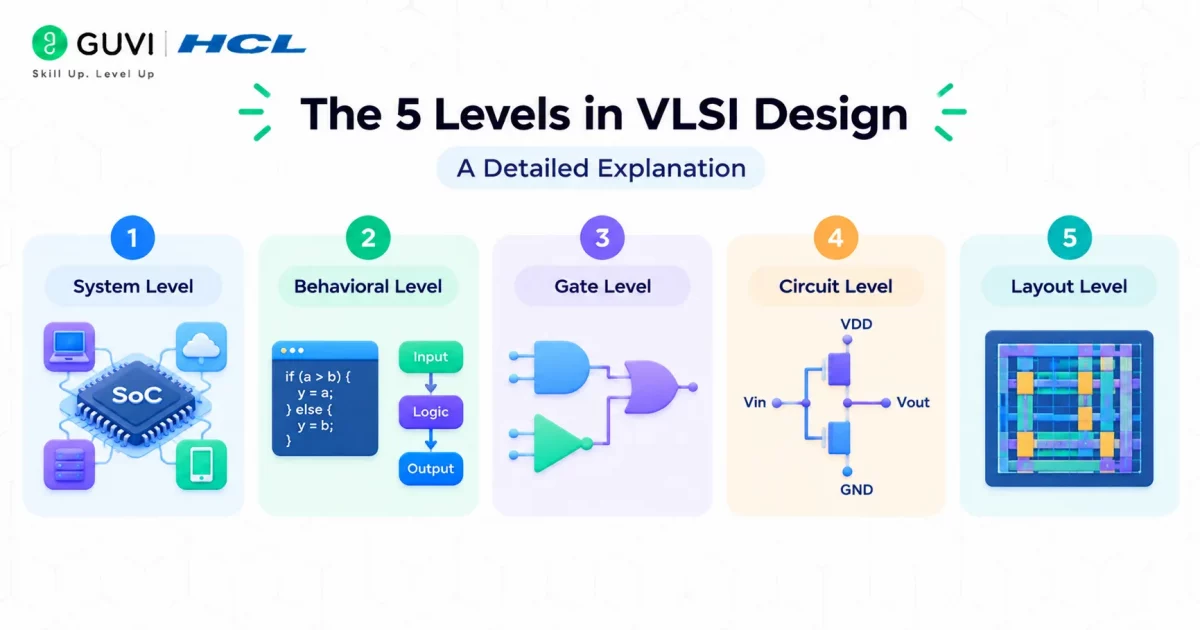
The VLSI design process follows five key levels: System, Behavioral, Gate, Circuit, and Layout. Understanding these levels helps you see how a chip moves from an initial concept to a complete physical component.
Table of contents
- TL;DR Summary
- What is VLSI Design?
- VLSI Design Levels Comparison: What Is Designed, Tools Used, and Skills Needed
- The 5 Levels in VLSI Design – A Detailed Explanation
- System Level
- Behavioral Level
- Gate Level
- Circuit Level
- Layout Level
- How Do These Levels in VLSI Design Work Together?
- Which VLSI Design Level Is Best for Freshers?
- Conclusion
- FAQs
- What is VLSI design?
- What are the main levels of VLSI design?
- What is the role of Hardware Description Languages (HDLs) in VLSI design?
- How does the physical design phase impact chip performance?
- What challenges are associated with VLSI design?
TL;DR Summary
- Levels in VLSI Design explain the complete process of transforming a chip from an idea into a manufacturable semiconductor device.
- The five Levels in VLSI Design are System Level, Behavioral Level, Gate Level, Circuit Level, and Layout Level, with each stage building on the previous one.
- Every level focuses on a different part of the design process and uses specific tools, design techniques, and engineering skills.
- Together, the Levels in VLSI Design help engineers design, verify, optimize, and prepare a chip for manufacturing.
- For freshers, Behavioral Level and Layout Level are generally the best starting points because they offer more entry-level opportunities.
- Understanding the Levels in VLSI Design helps build a strong foundation in semiconductor design, digital electronics, and modern chip development.
Carver Mead and Lynn Conway helped popularize modern VLSI design through their groundbreaking work in the 1970s.
What is VLSI Design?
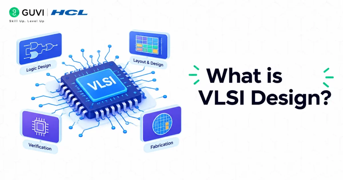
VLSI (Very Large Scale Integration) design is the process of integrating millions (or even billions) of transistors onto a single semiconductor chip.
This technique enables the creation of powerful processors, memory units, and specialized circuits used in nearly all modern electronic devices.
The VLSI design process is structured into five distinct levels, each focusing on a different aspect of chip development from conceptualization to the final physical layout. Let’s explore each level in detail in the coming sections.
Also Read: Why is VLSI Used?
If you want to learn VLSI design through a step-by-step process guided by a professional mentor, including Digital Electronics, UNIX and even Shell Scripting, consider enrolling in HCL GUVI’s Certified VLSI Design Course, which not only teaches you everything about the subject but also provides you with an industry-grade certificate!
VLSI Design Levels Comparison: What Is Designed, Tools Used, and Skills Needed
Before exploring each stage in detail, here’s a quick comparison of the Levels in VLSI Design. This table highlights what is designed at each level, the commonly used tools, and the skills required, making it easier to understand how each stage contributes to the overall chip design process:
| Level | What Is Designed | Tools Used | Skills Needed |
|---|---|---|---|
| System Level | Overall chip architecture, system functionality, major hardware blocks, and performance goals | MATLAB, Simulink, SystemC | System architecture, digital design fundamentals, system modeling, problem-solving |
| Behavioral Level | Chip behavior, data flow, and operations using HDL | Verilog, VHDL, ModelSim, Synopsys VCS, Xilinx Vivado | Verilog/VHDL, RTL design, functional simulation, debugging |
| Gate Level | Logic gate implementation and optimized gate-level netlists | Synopsys Design Compiler, Cadence Genus, Synopsys PrimeTime | Digital logic design, Boolean algebra, logic synthesis, timing analysis |
| Circuit Level | Transistor-level circuits and electrical implementation of logic gates | Cadence Virtuoso, SPICE, HSPICE, Synopsys Custom Compiler | CMOS design, transistor-level design, circuit analysis, analog and digital electronics |
| Layout Level | Physical chip layout, placement, routing, and design verification | Cadence Innovus, Synopsys IC Compiler II, Mentor Calibre, Cadence Pegasus | Physical design, floorplanning, placement & routing, DRC/LVS verification |
Build job-ready skills with HCL GUVI’s VLSI Design and Verification Course. Learn VLSI verification, simulation, static timing analysis, equivalence checking, and physical verification to design reliable, fabrication-ready circuits. Start building the skills the semiconductor industry demands.
The 5 Levels in VLSI Design – A Detailed Explanation
1. System Level
The System Level is the highest level of the VLSI design process. At this stage, engineers define what the chip should do before deciding how to build it. Instead of focusing on logic gates or transistors, they concentrate on the chip’s overall functionality, performance goals, power requirements, and major hardware blocks.
This level forms the foundation of the entire design. Decisions made here influence every stage that follows, so careful planning is essential.
What Happens at This Level?
- The chip’s purpose and functionality are defined.
- Major hardware blocks, such as CPU cores, memory, caches, communication interfaces, and I/O modules, are identified.
- Performance targets, power consumption, chip area, and cost requirements are established.
- The overall system architecture is planned, including how different blocks will communicate with one another.
- Different design approaches are evaluated to determine the most suitable architecture before implementation begins.
Key Tools Used
The exact tools vary depending on the company and project, but common tools include:
- MATLAB for algorithm development and system modeling.
- Simulink for modeling and simulating system behavior.
- SystemC for high-level system design and architectural exploration.
- Spreadsheet models, simulation frameworks, and custom analysis tools for estimating performance, power, and cost.
Example
A good real-world example is the design of the Apple M3. At the System Level, engineers first planned the chip’s overall architecture by deciding its major components, such as the CPU, GPU, memory system, and performance goals.
This high-level planning was completed before the detailed hardware design began.
2. Behavioral Level
Once the overall system has been planned, the next step is to describe how it should work. At the Behavioral Level, engineers define the chip’s behavior without worrying about the actual hardware implementation.
The goal is to make sure the design performs the required tasks correctly before it is converted into logic gates and circuits.
What Happens at This Level?
- Engineers specify the chip’s behaviour using Hardware Description Languages (HDLs) such as Verilog or VHDL.
- The movement of data and the sequence of operations are described.
- The design is simulated to check whether it produces the expected results.
- Different test cases are used to find and fix functional issues.
- Once the behavior is verified, the design is ready for the next stage of implementation.
Key Tools Used
Some of the most commonly used tools at this level include:
- Verilog and VHDL for describing hardware behavior.
- ModelSim for simulation and debugging.
- Synopsys VCS for functional verification.
- Xilinx Vivado for FPGA design and simulation.
Example
As we move from the System Level to the Behavioral Level, the design of the Apple M3 shifts from planning the overall architecture to describing how each hardware block should behave.
Engineers write this behavior using Verilog or VHDL and simulate the design to verify that it performs the required functions correctly before moving to the next level.
3. Gate Level
After the chip’s behavior has been verified, the design moves to the Gate Level. Here, the focus shifts from describing what the chip should do to showing how the hardware will perform those operations. The design is represented using digital logic gates, enabling the circuit to be implemented in hardware.
What Happens at This Level?
- The behavioral design is converted into a network of logic gates such as AND, OR, NOT, NAND, NOR, and XOR.
- The connections between these gates are defined to perform the required operations.
- The design is checked to ensure it still produces the correct outputs after conversion.
- Engineers optimize the gate-level design for speed, power consumption, and chip area.
- Timing analysis is performed to identify and fix delays that could affect performance.
Key Tools Used
Some commonly used tools at this stage include:
- Synopsys Design Compiler for logic synthesis.
- Cadence Genus for gate-level optimization and synthesis.
- Synopsys PrimeTime for timing analysis.
- Gate-level simulation tools for functional verification after synthesis.
Example
After verifying the behavior of the Apple M3, engineers convert the HDL design into logic gates. For example, operations performed by the processor’s Arithmetic Logic Unit (ALU) are implemented using thousands of interconnected gates.
At this stage, the design is optimized to meet the required performance, power, and area targets before moving to transistor-level implementation.
4. Circuit Level
At the Circuit Level, the design moves beyond logic gates and into the actual electronic circuits that make them work.

Every gate is built using transistors, and engineers ensure these circuits operate reliably under real electrical conditions. This stage focuses on the electrical behavior of the chip rather than its logical functions.
What Happens at This Level?
- Each logic gate is implemented using transistors, primarily CMOS technology.
- Electrical properties such as voltage, current, power consumption, and signal timing are analyzed.
- Engineers verify that the circuits function correctly under different operating conditions.
- Circuit designs are refined to improve speed, reduce power usage, and maintain stability.
- Detailed simulations are performed before the design is sent for physical layout.
Key Tools Used
The following tools are widely used during circuit design:
- Cadence Virtuoso for transistor-level circuit design.
- SPICE for circuit simulation and analysis.
- Synopsys Custom Compiler for custom circuit design.
- HSPICE for verifying circuit performance.
Example
Once the gate-level design of the Apple M3 is finalized, each logic gate is implemented using millions to billions of transistors.
Engineers simulate these transistor circuits to verify that they operate correctly, consume the expected amount of power, and meet the chip’s performance requirements before creating the physical layout.
5. Layout Level
The Layout Level is the final stage of the VLSI design process. By this point, the circuit design is complete, and engineers transform it into a physical layout that can be manufactured on a silicon wafer.
Every transistor, wire, and metal layer must be placed accurately so the chip functions as intended after fabrication.
What Happens at This Level?
- The chip is divided into distinct regions through floor planning.
- Standard cells and other components are placed in their designated locations.
- Metal wires are routed to connect all the components.
- Engineers perform Clock Tree Synthesis (CTS) to efficiently distribute the clock signal.
- The completed layout is verified using Design Rule Check (DRC) and Layout Versus Schematic (LVS) to ensure it is ready for manufacturing.
Key Tools Used
Some of the most commonly used tools at this stage are:
- Cadence Innovus for physical design and layout.
- Synopsys IC Compiler II for placement and routing.
- Mentor Calibre for DRC and LVS verification.
- Cadence Pegasus for physical verification.
Example
The final version of the Apple M3 reaches the Layout Level after its circuits have been fully designed and verified. Engineers carefully place billions of transistors, create the metal interconnections, and validate the complete layout before sending it to the semiconductor fabrication facility for manufacturing.
How Do These Levels in VLSI Design Work Together?
The Levels in VLSI Design are connected sequentially, with each level building on the work completed in the previous one. Instead of designing a chip all at once, engineers refine it step by step—from defining its overall purpose to creating a physical layout that can be manufactured.
Here’s how the process flows:
- System Level: Defines the chip’s overall architecture, functionality, and design goals.
- Behavioral Level: Describes how the chip should operate using hardware description languages such as Verilog or VHDL.
- Gate Level: Converts the behavioral design into interconnected logic gates and optimizes it for performance, power, and area.
- Circuit Level: Implements the logic gates using transistors and verifies their electrical behavior.
- Layout Level: Creates the chip’s physical layout by placing components, routing connections, and verifying the design is ready for manufacturing.
Every stage has a specific role, and together the levels in VLSI Design form the complete chip design process. Understanding how these levels work together helps students and aspiring VLSI engineers build a strong foundation in modern semiconductor design.
Which VLSI Design Level Is Best for Freshers?
If you’re starting a career in VLSI, it’s natural to wonder which design level offers the best entry point. The answer depends on your skills, interests, and the type of role you’re aiming for. While every level is important, some are more accessible to freshers than others.
For most beginners, the following areas offer the best opportunities:
- Behavioural Level (RTL Design): A great starting point for students familiar with Verilog, VHDL, digital electronics, and computer architecture. Many entry-level design roles begin at this level because it focuses on writing and verifying hardware behavior.
- Gate Level: Freshers with a strong understanding of digital logic, Boolean algebra, and logic synthesis can also find opportunities in gate-level design and verification.
- Layout Level (Physical Design): This is one of the most common entry points in the VLSI industry. Companies often hire fresh graduates for physical design, placement, routing, timing analysis, and layout verification roles after providing additional training.
The System Level is generally not an entry-level domain. It requires experience in system architecture, performance analysis, and making high-level design decisions. Similarly, the Circuit Level often demands a strong understanding of CMOS technology, transistor operation, and circuit design, making it more suitable for engineers with specialized knowledge.
If you’re a fresher looking to enter the VLSI industry, focusing on Behavioral Level (RTL Design) or Layout Level (Physical Design) usually provides the best career opportunities. Building a solid foundation in digital electronics, HDL programming, and VLSI design tools can significantly improve your chances of landing your first role.
Conclusion
In conclusion, VLSI design is a multi-layered process that transforms an initial idea into a working microchip. The five levels of VLSI design, Architectural, Functional, Logic, Circuit, and Physical work together to build efficient and powerful semiconductor devices.
Whether you’re an electronics student, an aspiring chip designer, or just curious about how microprocessors are made, mastering these VLSI design levels is a great starting point.
FAQs
1. What is VLSI design?
VLSI (Very Large Scale Integration) design involves integrating millions of transistors onto a single chip to create complex circuits, enabling the development of advanced electronic devices.
2. What are the main levels of VLSI design?
The primary levels include:
Architectural Design: Defining the system’s overall structure and functionality.
Functional Design: Describing the behavior of each component using hardware description languages.
Logic Design: Converting functional descriptions into specific logic circuits.
Circuit Design: Implementing logic circuits at the transistor level.
Physical Design: Mapping the circuit design onto the silicon chip.
3. What is the role of Hardware Description Languages (HDLs) in VLSI design?
HDLs, such as Verilog and VHDL, are used to model and describe the behavior of electronic systems, facilitating simulation and verification before physical implementation.
4. How does the physical design phase impact chip performance?
The physical design phase involves floorplanning, placement, and routing, which are crucial for meeting performance, area, and power consumption targets while adhering to manufacturing constraints.
5. What challenges are associated with VLSI design?
Challenges include managing process variations, adhering to stringent design rules, achieving timing closure, and ensuring first-pass silicon success due to the complexity and scale of modern integrated circuits.
Success Stories















Did you enjoy this article?