


VLSI Design Articles
What Does a 6-Month VLSI Program Curriculum from IIT Delhi Actually Teach You? We Break It Down
Semiconductors Explained: A Complete Guide to Modern Technology(2026)
High-Paying Jobs for Diploma Students in Semiconductor Industry in India
HCL GUVI for VLSI Training: Master Chip Design and Verification with Industry-Aligned Course


Get In Touch For Details! Request More Information
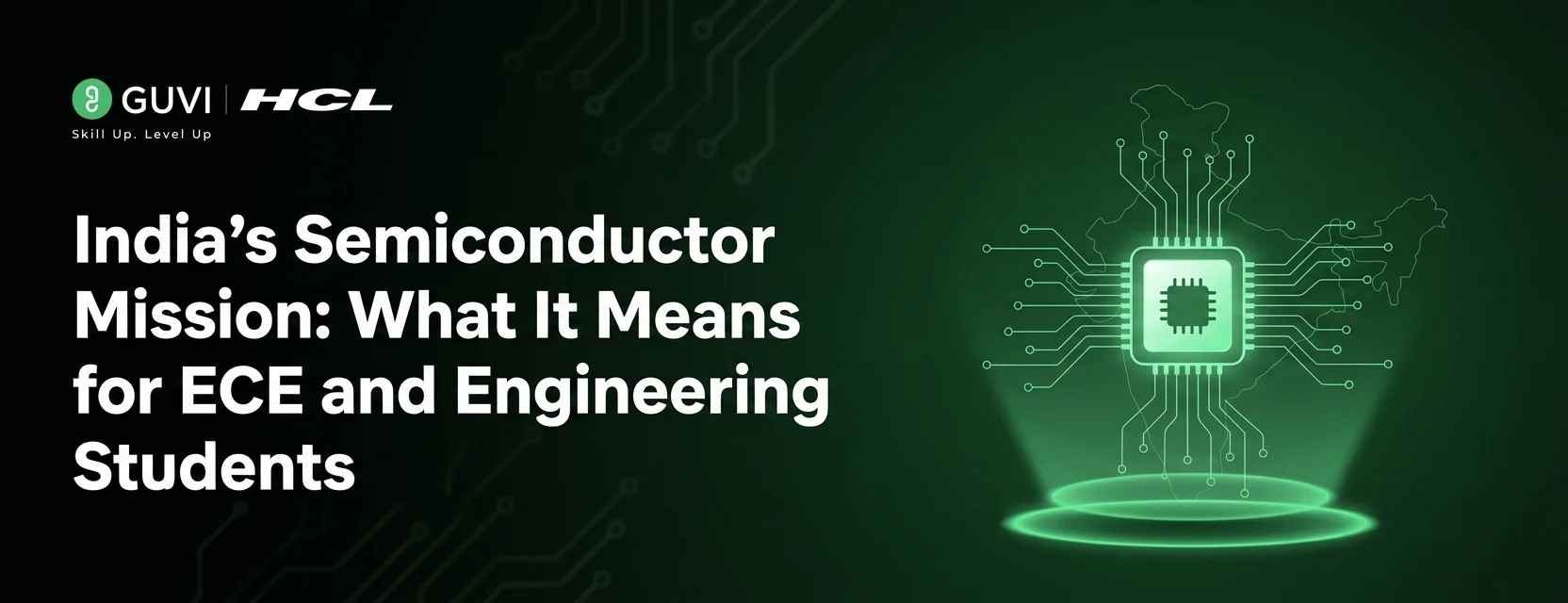
India’s Semiconductor Mission: What It Means for ECE and Engineering Students in 2026–2027
May 02, 2026 10 Min Read 2498 Views
(Last Updated)
TL;DR
- India’s Semiconductor Mission is a ₹76,000 crore initiative to build a full chip ecosystem in India
- Covers chip design, fabrication (fabs), OSAT, and display manufacturing
- Massive job creation across VLSI, verification, fabrication, and testing roles
- High demand for skills like Verilog, FPGA, SystemVerilog, and EDA tools
- Salaries are competitive due to a strong talent shortage
- Open to ECE, EEE, CS, and even diploma students
- Skill-based hiring is increasing, not just degree-based
- Major companies like Tata Electronics, Micron, and CG Power are actively investing and hiring
- Best time to start is now, before the competition increases
A quiet revolution is being assembled, not on the streets or in parliament, but inside clean rooms, design labs, and fabrication plants across India. The country is making one of the boldest industrial bets in its history: becoming a global force in semiconductor manufacturing and design.
If you’ve been following technology news in 2026, you’ve likely heard the phrase “India’s Semiconductor Mission” more than once. And for good reason.
With billions of dollars flowing into chip fabrication plants, design centers, and packaging units, India is rapidly reshaping its position in the global technology supply chain.
But here’s the question that matters most to you: What does this mean for your future?
If you’re an ECE, EEE, Computer Science, or even a diploma student, wondering where your career is headed, this could be the single biggest opportunity of your generation. The semiconductor industry is not just looking for IIT graduates or PhDs. It needs skilled, trained, and motivated engineers at every level. And India is building that ecosystem right now.
Read: Top 8 VLSI Design Job Roles
Table of contents
- What Is India's Semiconductor Mission?
- What Is India's Semiconductor Mission? A Complete Overview
- The Global Chip Shortage, That Made India's Semiconductor Mission Necessary
- Supply Chain Independence
- India's Push to Become a Global Electronics Hub
- India's Semiconductor Market: Key Statistics
- 8 Key Ways India's Semiconductor Mission Benefits Students
- Explosion of Job Opportunities
- High-Demand Skill Sets
- Entry Opportunities for Diploma Students
- Growth of VLSI and Chip Design Careers
- More Internships and Industry Exposure
- Rise of Semiconductor Startups
- Better Salaries and Career Growth
- Opportunities Without a Coding Background
- Where Are India's Semiconductor Mission Jobs Located?
- Gujarat: The Fabrication Hub
- Karnataka: The Design Capital
- Telangana: The Emerging Design Hub
- Tamil Nadu: Manufacturing and Design
- Other Notable Locations
- Top Companies Investing Under the Mission
- Skills Students Need to Succeed in India's Semiconductor Mission Ecosystem
- Best Courses and Certifications for Semiconductor
- How to Prepare for a Career in India's Semiconductor Mission
- Challenges Students Should Be Aware Of
- Future Scope of India's Semiconductor Industry
- Conclusion
- Frequently Asked Questions
- What is India's Semiconductor Mission?
- Which companies are hiring under India's Semiconductor Mission?
- Is semiconductor a good career for ECE students in India in 2025?
- What is the salary for a VLSI engineer fresher in India?
- Can diploma students get jobs in the semiconductor industry?
- What skills are needed to get a semiconductor job in India?
- What is the C2S program by MeitY?
- Which city in India has the most semiconductor jobs?
- Do I need coding skills for semiconductor jobs?
- How do I start preparing for a semiconductor career as an engineering student?
What Is India’s Semiconductor Mission?
India’s Semiconductor Mission (ISM) is a government-led initiative launched under the India Semiconductor Mission program, backed by the Ministry of Electronics and Information Technology (MeitY). The mission was formally established with a budget of ₹76,000 crore (approximately $10 billion USD) to build a robust and sustainable semiconductor and display manufacturing ecosystem within India.
The mission is structured around four core focus areas:
- Chip Fabrication (Fabs): Building facilities that manufacture semiconductor wafers, the physical chips that power every electronic device.
- Chip Design: Supporting companies and talent that design the logic, circuits, and architecture of chips.
- OSAT (Outsourced Semiconductor Assembly and Testing): Setting up packaging and testing units, which are critical steps after fabrication.
- Display Fabrication: Manufacturing panels for screens and displays, which rely on similar technologies.
Explore: Top Highest Paying Engineering Jobs in India
The goal is not merely to assemble imported chips; India wants to own significant portions of the semiconductor value chain, from design all the way to packaging and testing. This is a structural, long-term shift in India’s industrial policy, and the investments being made today will generate careers for decades.
Ready to enter India’s Semiconductor Mission workforce?
HCL GUVI VLSI Design & Verification Course is built specifically for ECE and EEE students targeting the semiconductor industry.
India Semiconductor Mission: Key Milestones (2022–2030)
| Year | Milestone |
| 2020–2022 | Global chip shortage exposes supply chain vulnerability worldwide |
| 2022 | India’s Semiconductor Mission (ISM) formally launched with ₹76,000 crore budget |
| 2023 | Micron Technology receives approval for OSAT facility in Sanand, Gujarat |
| 2023 | C2S (Chips to Startup) program launched by MeitY to fund chip design initiatives |
| 2024 | Tata Electronics, PSMC fab groundbreaking in Dholera, Gujarat |
| 2024 | CG Power and Kaynes Semiconductor receive approvals under ISM |
| 2025–2026 | Hiring ramp-up begins across fab, OSAT, and design center projects |
| 2027–2028 | India’s first commercial fab expected to begin production |
| 2030 | Domestic semiconductor market projected to reach $100 billion (IESA) |
Read: How to learn the VLSI Course from Scratch? 12 Steps to Follow

What Is India’s Semiconductor Mission? A Complete Overview
The timing of this mission is no accident. Several converging forces made 2022–2026 the right moment for India to act decisively.
The Global Chip Shortage, That Made India’s Semiconductor Mission Necessary
Between 2020 and 2022, the world experienced a catastrophic semiconductor shortage. Automobile factories shut down. Consumer electronics were delayed. Billions of dollars in economic value were lost, all because of a shortage of chips that are often smaller than a fingernail. Countries that depended entirely on Taiwan, South Korea, and China for their chip supply suddenly found themselves vulnerable.
India, which was rapidly growing its electronics consumption, realized it could not afford to remain dependent. The shortage exposed a critical strategic weakness: no chips meant no products, no cars, no phones, and no growth.
Supply Chain Independence
Geopolitical tensions, particularly those involving China and Taiwan, pushed governments worldwide to rethink supply chains. The United States passed the CHIPS Act.
Europe launched its own Chips Act. Japan, South Korea, and others doubled down on domestic manufacturing. India recognized that if it wanted to be a serious economic power, it needed to secure its semiconductor supply chain.
India’s Push to Become a Global Electronics Hub
India already has massive advantages: a large pool of engineering graduates, a growing domestic electronics market, competitive land and labour costs, and significant government willingness to offer production-linked incentives (PLI).
The Semiconductor Mission is the keystone that can turn India from an electronics consumer into an electronics producer and, eventually, a global chip supplier.
Quote
India’s Semiconductor Market: Key Statistics
- Government investment: ₹76,000 crore (~$10B USD) under ISM
- Direct jobs expected (short-term): 20,000+ skilled positions
- Indirect employment (over the next decade): Hundreds of thousands
- Domestic semiconductor market by 2030: $100 billion (Source: IESA)
- India’s current global chip output contribution: ~1% (growing)
- Design center cities: Bangalore, Hyderabad, Pune, already home to Intel, Qualcomm, TI, ARM
8 Key Ways India’s Semiconductor Mission Benefits Students
1. Explosion of Job Opportunities
The most immediate and visible impact of the Semiconductor Mission is job creation, and the numbers are significant.
Approved projects from companies such as Tata Electronics, Micron Technology, and CG Power are expected to directly create over 20,000 skilled jobs in the short term, with indirect employment in the hundreds of thousands over the next decade.
What does this mean in practice? New categories of roles are emerging rapidly:
- VLSI Design Engineers: designing the logic and circuits of chips
- Physical Design Engineers: translating logic designs into physical layouts
- Verification Engineers: ensuring chips perform exactly as intended
- Fab Technicians: operating and maintaining fabrication equipment
- Test Engineers: validating chips post-production
- Process Engineers: optimizing manufacturing processes
Many of these roles did not exist at scale in India just five years ago. Today, they represent a genuine career path with competitive salaries and long-term stability.
2. High-Demand Skill Sets
One of the most significant shifts the Semiconductor Mission is accelerating is the move from degree-based hiring to skill-based hiring.
Companies are not just looking for graduates from tier-1 institutions. They are looking for engineers who can demonstrate working knowledge of:
- HDL Languages: Verilog and VHDL for digital design
- FPGA Design and Implementation
- Physical Design Tools: Cadence, Synopsys, Mentor Graphics
- Simulation and Verification: SystemVerilog, UVM testbenches
- Analog and Mixed-Signal Design
The talent gap in India’s semiconductor sector is real and significant. This means that students who proactively build these skills, regardless of their college rank, will find genuine, well-paying opportunities. A student from a tier-3 college with solid Verilog skills and a project portfolio can genuinely compete with graduates from top institutions.
Don’t know where to start with Verilog, FPGA, or EDA tools?
HCL GUVI VLSI Design & Verification Course covers every skill companies under India’s Semiconductor Mission are hiring for, from RTL design to verification, with live mentorship and real project experience.
3. Entry Opportunities for Diploma Students
A common misconception is that the semiconductor industry is only for B.Tech or M.Tech holders. The reality is very different.
Fabrication plants and OSAT facilities require large numbers of trained technicians, roles perfectly suited for diploma holders in Electronics, Electrical, Mechanical, and even Chemical Engineering. These roles involve:
- Operating and monitoring fab equipment
- Maintaining cleanroom environments
- Performing quality checks and basic testing
- Assisting process engineers in production lines
This is a genuine opportunity for polytechnic and ITI graduates to enter a cutting-edge, well-paying industry. Companies like Micron’s OSAT facility in Gujarat have explicitly highlighted the need for technician-level talent. If you hold a diploma and have strong fundamentals, do not count yourself out of this wave.
4. Growth of VLSI and Chip Design Careers
India has quietly been a significant player in chip design for years; companies like Intel, Qualcomm, Texas Instruments, and ARM have large design centers in Bangalore, Hyderabad, and Pune. The Semiconductor Mission is now accelerating this trend dramatically.
With domestic fabrication facilities coming online, there is a growing need for design engineers who can create chips specifically for Indian applications, in defence, automotive, telecom, and consumer electronics.
This means:
- More hiring for fresh graduates in VLSI design roles
- Growing demand for physical design, DFT (Design for Testability), and timing closure expertise
- Expanded opportunities in analog and RF design for wireless communication
- India increasingly becoming the preferred destination for global semiconductor companies to set up design teams
If you are interested in chip design, the next five years in India could offer opportunities comparable to what Silicon Valley offered engineers in the 1990s.
VLSI and chip design careers are growing faster than ever under India’s Semiconductor Mission. If you want to enter this space as a fresh graduate, the right training makes all the difference.
HCL GUVI VLSI Design & Verification Course is designed to take you from zero to job-ready, with a curriculum aligned to what Tata, Micron, and top design centers are actively hiring for.
5. More Internships and Industry Exposure
One of the structural problems in India’s engineering education has been the gap between what colleges teach and what industries need. The Semiconductor Mission is beginning to address this directly.
Government-backed programs and private sector initiatives are driving:
- Industry-academia collaborations between colleges and semiconductor companies
- Funded internship programs placing students inside design centers and fab facilities
- Curriculum updates aligned with real industry tools and workflows
- Chip design labs being established in universities through programs like C2S (Chips to Startup) by MeitY
For students, this means a growing number of opportunities to gain real-world exposure before graduation, which is exactly what makes a resume stand out in a competitive hiring market.
6. Rise of Semiconductor Startups
Not all opportunities in the semiconductor ecosystem come through large corporations. The Indian government is actively funding and supporting semiconductor startups through initiatives like:
- The C2S (Chips to Startup) Program , funding chip design from concept to fabrication
- Startup India incentives for electronics and deep tech ventures
- IESA (India Electronics and Semiconductor Association) ecosystem support
This opens up an entirely different career path: joining an early-stage chip design startup, contributing to a niche product, and growing with the company. Some of India’s most exciting career stories in the next decade will come not from MNCs but from startups that were founded because of the infrastructure and incentives the Semiconductor Mission has created.
For students with an entrepreneurial mindset, this is a genuine opportunity to build something from the ground up.
7. Better Salaries and Career Growth
Supply and demand govern salaries, and right now, the demand for semiconductor talent in India significantly outpaces supply. This has a very direct consequence: competitive, often premium salaries.
Fresh graduates with VLSI or physical design skills are commanding packages that, just three years ago, would have required two to three years of experience. As more fabs and design centers come online, this talent shortage is unlikely to resolve quickly, which means:
- Starting salaries in VLSI roles typically range from ₹6–12 LPA for fresh graduates, with experienced engineers earning significantly more
- Professionals with 5–8 years of specialized experience are among the most sought-after in India’s tech job market
- Career progression is accelerated because companies are building teams rapidly and need people to grow into leadership roles quickly
If long-term financial stability and upward mobility matter to your career planning, and they should, semiconductors represent one of the strongest bets you can make right now.
8. Opportunities Without a Coding Background
Here is something that surprises many students: you do not need to be a software developer to thrive in the semiconductor industry.
In fact, a significant share of semiconductor roles are hardware-focused and require very little traditional programming. These include:
- Layout Engineers: manually drawing or verifying the physical layout of chip components
- Test and Validation Engineers: running tests on fabricated chips using specialized equipment
- Failure Analysis Engineers: diagnosing why chips fail under certain conditions
- Process Integration Engineers: working on the chemical and physical processes inside fabs
- Package Design Engineers: designing how chips are encased and connected to circuit boards
For students who struggled with software development but have strong fundamentals in electronics, physics, or materials, the semiconductor industry is actively looking for you. The notion that all high-paying tech careers require Python or Java skills simply does not apply here.
Where Are India’s Semiconductor Mission Jobs Located?
The Semiconductor Mission has created distinct geographic clusters. Knowing where to look and being open to relocation significantly broadens your opportunities.
Gujarat: The Fabrication Hub
- Sanand: Micron OSAT facility, CG Power OSAT, Kaynes Semiconductor OSAT
- Dholera: Tata Electronics–PSMC fab (India’s first commercial chip fabrication plant)
- Best suited for: Fab technicians, process engineers, test engineers, and OSAT roles
Karnataka: The Design Capital
- Bangalore: Intel, Qualcomm, Texas Instruments, ARM, Broadcom design centers
- India’s most mature semiconductor design ecosystem
- Best suited for: VLSI design, physical design, verification, analog design
Telangana: The Emerging Design Hub
- Hyderabad: Growing design center presence; government push for semiconductor clusters
- Best suited for: Design and verification roles, startup opportunities
Tamil Nadu: Manufacturing and Design
- Chennai: Electronics manufacturing base; growing semiconductor ecosystem
- Coimbatore: Emerging as a talent feeder city for semiconductor companies
- Best suited for: Electronics manufacturing, embedded hardware, test roles
Other Notable Locations
- Pune (Maharashtra): Design centers for automotive semiconductors
- Delhi-NCR: Embedded systems and defense semiconductor roles
Top Companies Investing Under the Mission
Several major domestic and international players have made concrete, approved commitments under India’s Semiconductor Mission:
Micron Technology is setting up an OSAT (assembly and testing) facility in Sanand, Gujarat, a multi-billion-dollar investment that will create direct and indirect employment on a significant scale. This marks one of the largest semiconductor investments by a US company in India.
Tata Electronics, in partnership with Taiwan’s Powerchip Semiconductor Manufacturing Corp (PSMC), is building a semiconductor fabrication plant in Dholera, Gujarat, India’s first commercial fab for chips.
CG Power (in partnership with Renesas Electronics and Stars Microelectronics) is setting up an OSAT facility in Sanand, Gujarat.
Kaynes Semiconductor is building an OSAT facility in Sanand, one of the first domestic Indian semiconductor companies to receive approval under the mission.
For students, this means that these companies will need to hire engineers, technicians, and managers at multiple levels over the coming years. Keeping a close watch on their hiring pipelines and building skills aligned with their requirements is a genuinely practical career strategy.
Skills Students Need to Succeed in India’s Semiconductor Mission Ecosystem
You do not need to wait for the fab to open to begin preparing. The best time to build semiconductor skills is right now, while competition is still relatively low and resources are more accessible than ever.
Core Electronics Fundamentals Revisit your basics: digital logic, analog circuits, semiconductor physics, signals, and systems. Strong fundamentals are non-negotiable and differentiate serious candidates from those who have only surface-level exposure.
Hardware Description Languages (HDL) Start with Verilog, it is the most widely used HDL in the industry. Learn to write RTL (Register Transfer Level) code, simulate it, and synthesize it. Move to VHDL as a secondary skill. Practice on platforms like HDLBits, which offers free, structured Verilog exercises.
FPGA Tools and Platforms FPGAs are the closest accessible hardware to professional chip design. Learn to use Xilinx Vivado or Intel Quartus, both offer free versions. Building an FPGA project (a UART controller, a simple processor, or a signal processing block) is one of the most powerful things you can put in your portfolio.
Simulation and EDA Tools Familiarize yourself with tools like ModelSim, Cadence Xcelium, or Synopsys VCS for simulation. Many of these have student licenses or free tiers.
Soft Skills That Matter Semiconductor work is highly collaborative and detail-oriented. Problem-solving discipline, the ability to read and interpret datasheets and specifications, and systematic debugging skills are consistently flagged by hiring engineers as differentiators.
Best Courses and Certifications for Semiconductor
| Platform / Program | Course / Resource | Cost | Best For |
| NPTEL | Digital Circuits, VLSI Design, Analog Electronics | Free | All students |
| HDLBits | Verilog Practice Exercises | Free | Verilog beginners |
| MeitY C2S Program | Chips to Startup , Funded chip design | Funded (apply) | |
| Maven Silicon | VLSI Design, Physical Design Courses | Paid | Job-focused VLSI training |
| HCL GUVI VLSI Course | Industry-integrated VLSI Design, RTL Placement Support | Paid | ECE/EEE students targeting ISM jobs |
| Coursera | VLSI CAD by UIUC, Hardware Security | Paid / Free | Structured learning |
| Udemy | Verilog / FPGA / SystemVerilog courses | Paid / Free | Self-paced learners |
| Intel Quartu | Intel FPGA University Program | Free | FPGA design practice |
How to Prepare for a Career in India’s Semiconductor Mission
Here is a practical roadmap you can begin following today, regardless of which year you are in:
Step 1: Strengthen Your Fundamentals (3–6 months) Focus on digital electronics, analog circuits, and semiconductor physics. Use NPTEL courses, which are free and high quality. Make sure you can explain how a MOSFET works, what setup and hold time means, and how a flip-flop operates.
Step 2 : Learn Verilog and Build Projects (3–6 months) Complete a structured Verilog course, then build 2–3 projects of increasing complexity. Publish them on GitHub. This project portfolio is your most powerful job application asset.
Step 3 : Get Hands-On with FPGA (2–4 months) Implement your Verilog designs on an actual FPGA board (the Basys 3 or Nexys A7 are affordable and widely supported). Document your work.
Step 4 : Pursue Targeted Certifications Look at courses from platforms like Maven Silicon, VLSIGuru, Udemy (for Verilog/FPGA), or Coursera (for broader electronics). The C2S program from MeitY also offers funded opportunities for eligible students.
Step 5 : Apply for Internships Early Target internships at semiconductor design companies , both large MNCs and startups. Even a two-month internship where you work with real tools adds enormous credibility to your profile.
Step 6 : Stay Current Follow industry publications like SemiEngineering, EE Times India, and Electronics For You. Understanding industry trends makes you a more informed, more attractive candidate.
Instead of piecing together free resources across multiple platforms, HCL GUVI VLSI Design & Verification Course gives you a structured, mentor-guided path through Verilog, SystemVerilog, and verification, exactly the skills India’s Semiconductor Mission companies are hiring for right now.
Challenges Students Should Be Aware Of
Honest career guidance requires acknowledging the obstacles alongside the opportunities.
The Skill Gap Is Real: And It Is Your Responsibility Colleges are improving, but many curricula still lag significantly behind industry needs. Do not assume a degree alone will open doors. You must supplement your formal education with self-directed learning. The gap between what is taught and what is needed is your opportunity; bridge it before someone else does.
Continuous Learning Is Not Optional. Semiconductors is a rapidly evolving field. New process nodes, new tools, new architectures, the learning never stops. Students who thrive in this industry are those who develop a genuine curiosity for how things work and a habit of continuous self-improvement.
The Environment Is Competitive As the industry grows in India, so will the number of students trying to enter it. Being early is an advantage, but only if you use that time wisely. Solid fundamentals, demonstrable skills, and real projects will consistently outperform vague credentials.
Geographic Flexibility May Be Required. Major semiconductor clusters are emerging in Gujarat (Sanand, Dholera), Karnataka (Bangalore), Telangana (Hyderabad), and Tamil Nadu. Students willing to relocate will have significantly broader access to opportunities.
Future Scope of India’s Semiconductor Industry
Where is all of this heading?
India’s semiconductor industry today is nascent. The country contributes roughly 1% of global semiconductor output, a figure that will grow substantially over the next decade, but requires context: even reaching 5–10% would represent a massive economic and employment transformation.
The India Electronics and Semiconductor Association (IESA) estimates the domestic semiconductor market will reach $100 billion by 2030. Global analysts see India becoming a meaningful alternative to China for semiconductor supply chains , particularly for assembly, testing, and increasingly for design.
Long-term, the roles that will define India’s semiconductor future include:
- AI Chip Design: custom silicon for machine learning and inference
- Automotive Semiconductors : chips for EVs, ADAS, and connected vehicles
- IoT and Edge Computing Chips: low-power designs for smart devices
- Photonics and Advanced Packaging : next-generation chip interconnect technologies
For students entering the industry today, the trajectory points toward long-term relevance. Unlike software fields that see rapid commoditisation, semiconductor engineering, particularly design and process engineering, remains a highly specialized, intellectually demanding, and well-compensated discipline for decades.
Conclusion
India’s Semiconductor Mission is not just an industrial policy. It is a generational opening, one that has not existed at this scale for Indian engineering students before.
The ecosystem being built right now will require engineers, technicians, designers, and innovators at every level. It will create careers that are technically challenging, financially rewarding, and strategically important to the country. It will produce India’s own chip companies, its own design IP, and eventually its own fabrication capability at global standards.
But opportunity does not wait. The students who will benefit most are those who begin preparing today, while the industry is still being built, before the competition intensifies, and while skill-based differentiation still carries disproportionate reward.
Frequently Asked Questions
What is India’s Semiconductor Mission?
India’s Semiconductor Mission (ISM) is a government initiative backed by MeitY with a budget of ₹76,000 crore (~$10 billion USD). Its goal is to build a domestic semiconductor and display manufacturing ecosystem in India, covering chip fabrication, OSAT, design, and display manufacturing.
Which companies are hiring under India’s Semiconductor Mission?
Major companies with approved projects include Micron Technology (OSAT, Gujarat), Tata Electronics in partnership with PSMC (Fab, Gujarat), CG Power with Renesas (OSAT, Gujarat), and Kaynes Semiconductor (OSAT, Gujarat). Global design centers from Intel, Qualcomm, ARM, and Texas Instruments in Bangalore and Hyderabad are also hiring.
Is semiconductor a good career for ECE students in India in 2025?
Yes, it is one of the strongest career options for ECE students right now. Demand for VLSI and semiconductor talent significantly outpaces supply in India, resulting in strong starting packages (₹6–12 LPA for fresh graduates) and fast career growth. The sector is expected to grow substantially through 2030 and beyond
What is the salary for a VLSI engineer fresher in India?
Fresh graduates with VLSI or physical design skills typically earn between ₹6 LPA and ₹12 LPA at entry level. Engineers with 5–8 years of specialized experience are among the most highly compensated in India’s tech industry.
Can diploma students get jobs in the semiconductor industry?
Yes. OSAT and fabrication facilities require a large number of trained technicians — roles well-suited for diploma holders in Electronics, Electrical, Mechanical, or Chemical Engineering. Companies like Micron’s Gujarat facility have explicitly highlighted demand for technician-level talent.
What skills are needed to get a semiconductor job in India?
Key skills include: Verilog / VHDL (HDL languages), FPGA design and implementation, EDA tools (Cadence, Synopsys, Mentor Graphics), simulation tools (ModelSim, Xcelium), and strong fundamentals in digital and analog electronics. Soft skills like systematic debugging and datasheet reading are also highly valued.
What is the C2S program by MeitY?
The Chips to Startup (C2S) program is a MeitY initiative that provides funded access to chip design tools, resources, and training to colleges and students in India. Its goal is to develop 85,000 skilled engineers in the semiconductor sector. Eligible students can access EDA tools and chip design programs at little to no cost.
Which city in India has the most semiconductor jobs?
Bangalore currently has the highest concentration of semiconductor design jobs in India, home to large design centers from Intel, Qualcomm, ARM, Texas Instruments, and Broadcom. For fabrication and OSAT roles, Gujarat (Sanand and Dholera) is rapidly emerging as the primary hub.
Do I need coding skills for semiconductor jobs?
Not necessarily. Many semiconductor roles are hardware-focused: layout engineers, test engineers, failure analysis engineers, process integration engineers, and package design engineers require very little traditional software programming. A strong background in electronics, physics, or materials science is often more relevant.
How do I start preparing for a semiconductor career as an engineering student?
Start by strengthening your fundamentals in digital and analog electronics. Then learn Verilog via free resources like HDLBits, build 2–3 FPGA projects, and explore free courses on NPTEL and Coursera. Apply for internships early, and consider specialized training through Maven Silicon or VLSIGuru for job-focused preparation.
Success Stories

About the Author
Salini Balasubramaniam
A curious, information-savvy writer loves to turn deep insights into authentic and engaging content that connects. With experience in writing for brands and driving audience engagement, I believe that words can make a powerful difference.
View all posts by Salini Balasubramaniam
Connect with me @


Did you enjoy this article?