

VLSI Design Articles
Why Chips Fail: A Basic Guide to Chip Defects and IC Failure Analysis
Fun Facts About the Semiconductor Industry
Why Are Semiconductor Chips Expensive? Manufacturing Cost Explained
Instruction Set Architecture: How ISA Shapes Modern Chip Design
Get In Touch For Details! Request More Information
How HCL GUVI’s VLSI Design Program Prepares You for the Semiconductor Industry
Aug 03, 2026 2 Min Read 279 Views
(Last Updated)
The semiconductor industry is one of the fastest-growing, highest-paying tech sectors right now, and VLSI design talent is in short supply. If you’ve been considering a serious, credential-backed entry into chip design, here’s a program worth exploring: the IIT Delhi Certified Program in Digital VLSI Design (Batch 2), offered by CEP, IIT Delhi in association with HCL GUVI.
Table of contents
- About the Course
- Course Content & Syllabus
- Tools & Technologies
- Projects Implemented
- Price & Duration
- Certificates & Benefits
- Why This Program Stands Out
- Final Thoughts
- 🚀 Ready to build your semiconductor career?
- FAQs
- Q1. Who offers this programme?
- Q2. What's the course duration and schedule?
- Q3. Who can apply?
- Q4. What's the programme fee?
- Q5. What certificate will I receive?
- Q6. Is there a campus component?
About the Course
This is a live, faculty-led program delivered directly by IIT Delhi professors, covering the complete RTL-to-GDSII digital VLSI design flow — from CMOS fundamentals to physical design and low-power methodologies. It’s built for working professionals, graduates, and job seekers from Electronics, Electrical, Physics, or Computer Science backgrounds, with live sessions every Sunday.
Course Content & Syllabus
The curriculum spans 8 in-depth modules covering the full chip design lifecycle:
- Digital IC Design (CMOS ASIC design flow, MOS device physics, logic gates)
- Scripting for VLSI Professionals (Linux, VLSI scripting, RTL coding & design styles)
- Logic Synthesis & STA (synthesis optimization, static timing analysis, power-aware synthesis)
- Design for Testability & Reliability (scan chain insertion, ATPG & BIST, fault models)
- Physical Design (floorplanning, placement & routing, CTS, advanced node challenges)
- Low Power & Advanced Design Techniques (low power methodologies, UPF/CPF)
- Mixed-Signal & AMS Design (analog IC design, PLL & clock generation circuits)
- Packaging in VLSI
Tools & Technologies
You’ll build practical, industry-relevant skills across:
- Linux (scripting environment)
- RTL coding & VLSI design flow tools
- EDA tools for synthesis, STA & physical design
- ATPG & BIST tools for testability
- UPF/CPF frameworks for power-aware design
Projects Implemented
You’ll apply concepts through hands-on VLSI design challenges, including:
- Combinational and Sequential CMOS Circuit Design
- Low Power I/O Circuit Design
- Power Management IC (PMIC) Design
- Clock Tree Synthesis and Static Timing Analysis
- Design for Test (DFT) and Automatic Test Pattern Generation
Price & Duration
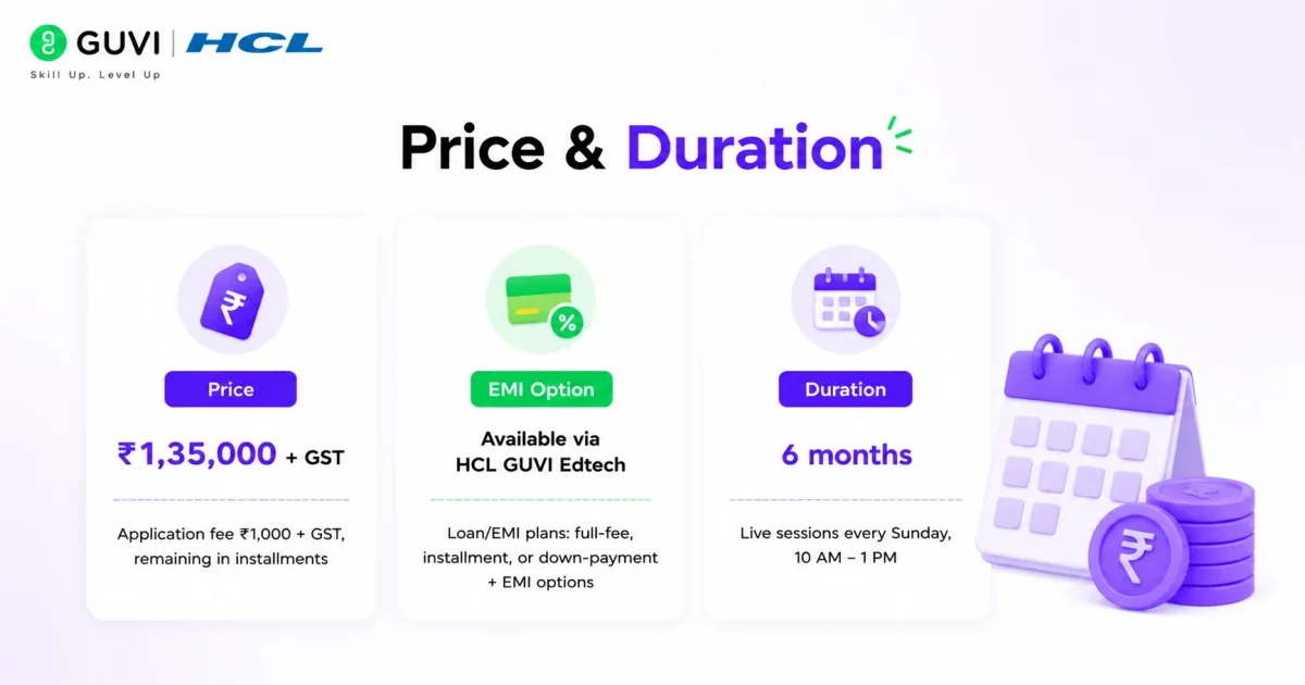
- Price: ₹1,35,000 + GST (application fee ₹1,000 + GST, remaining in installments)
- EMI Option: Available via HCL GUVI Edtech (loan/EMI plans; full-fee, installment, or down-payment + EMI options)
- Duration: 6 months (live sessions every Sunday, 10 AM–1 PM)
Certificates & Benefits
- e-Certificate of Completion from CEP, IIT Delhi (for 60%+ score & 50%+ attendance)
- e-Certificate of Participation (for 50%+ attendance)
- 3-day campus immersion at IIT Delhi (optional; travel & stay self-funded)
- Direct guidance from IIT Delhi faculty
- Group project & peer-to-peer learning
- Access to session recordings for the programme duration
- ₹10,000 Amazon voucher on successful referrals

Why This Program Stands Out
Unlike most VLSI courses that focus on isolated tools, this program covers the entire RTL-to-GDSII flow with direct instruction from IIT Delhi faculty — professors with research backgrounds from Intel, Texas Instruments, Global Foundries, and international institutions like NUS and Tyndall National Institute. Add a campus immersion and peer-to-peer learning, and you get an academic depth most bootcamps simply can’t match.
Final Thoughts
VLSI and semiconductor design is a specialized, high-value career path, and this program gives you a structured, IIT Delhi-backed route into it — whether you’re an aspiring chip designer, a working engineer looking to upskill, or a fresh graduate from an electronics background.
🚀 Ready to build your semiconductor career?
Applications close 24th July 2026, with the programme starting 26th July 2026 — seats are limited and filling fast.
👉 Apply for the IIT Delhi Digital VLSI Design Programme Now!
FAQs
Q1. Who offers this programme?
The Continuing Education Programme (CEP), IIT Delhi, in association with HCL GUVI.
Q2. What’s the course duration and schedule?
6 months, with live online sessions every Sunday from 10 AM to 1 PM IST.
Q3. Who can apply?
Graduates or diploma holders from Electronics, Electrical, Physics, or Computer Science backgrounds; working professionals and fresh graduates are both eligible.
Q4. What’s the programme fee?
₹1,35,000 + GST, with a ₹1,000 + GST non-refundable application fee and the balance payable in installments.
Q5. What certificate will I receive?
An e-Certificate of Completion or Participation from CEP, IIT Delhi, based on attendance and evaluation criteria.
Q6. Is there a campus component?
Yes — an optional 3-day immersion at the IIT Delhi campus (travel and accommodation self-funded).
Success Stories

About the Author
Isha Sharma
I’m a versatile technical content writer with over 3.5 years of experience in technical writing and 1 year of experience in web development. My specialized domains are web development, AWS, cloud computing, etc. I have written over 250+ SEO-optimized technical articles.
View all posts by Isha Sharma
Connect with me @








Did you enjoy this article?