


VLSI Design Articles
Why Chips Fail: A Basic Guide to Chip Defects and IC Failure Analysis
Fun Facts About the Semiconductor Industry
Why Are Semiconductor Chips Expensive? Manufacturing Cost Explained
Instruction Set Architecture: How ISA Shapes Modern Chip Design


Get In Touch For Details! Request More Information
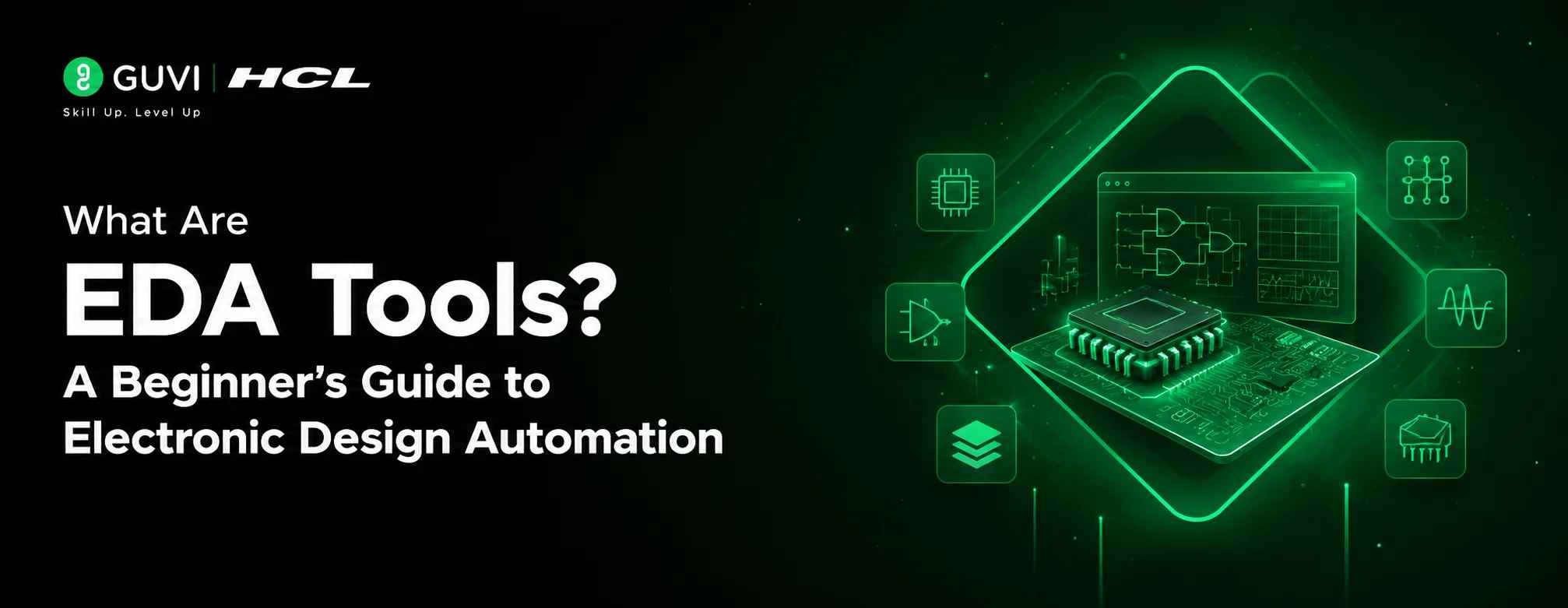
What Are EDA Tools? A Beginner’s Guide to Electronic Design Automation
Jul 21, 2026 6 Min Read 728 Views
(Last Updated)
Table of contents
- TL;DR Summary
- Introduction
- What Are EDA Tools?
- What are EDA tools?
- Why beginners should care
- Why Are EDA Tools Important in Semiconductor Design?
- They reduce manual design errors
- They improve first-pass silicon success
- They support faster product launches
- How EDA Tools Work in a Chip Design Flow
- Step 1: Specification and architecture
- Step 2: RTL design
- Step 3: Simulation and verification
- Step 4: Synthesis
- Step 5: Physical design and signoff
- EDA Tools List: Common Categories and Examples
- Common EDA tool categories
- Popular EDA software examples
- EDA Tools vs CAD Tools in VLSI
- EDA Tools in Action : Practical Examples
- Example 1: AI chip companies
- Example 2: Automotive electronics
- Example 3: PCB and package design
- Career Benefits of Learning EDA Tools
- Skills to Build First Before Learning EDA Tools
- Digital Electronics
- Verilog or SystemVerilog
- Basic Linux Commands
- RTL Simulation
- Timing Concepts
- Synthesis Basics
- PCB or VLSI Project Practice
- Common Mistakes Beginners Make
- Mistake 1: Learning tools without digital design basics
- Mistake 2: Ignoring verification
- Mistake 3: Confusing simulation with synthesis
- Mistake 4: Not building projects
- Mistake 5: Skipping documentation
- Wrapping Up
- Frequently Asked Questions
- What are EDA tools?
- Why are EDA Tools important in VLSI?
- Is EDA software only used for chip design?
- What is the difference between EDA tools and CAD tools in VLSI?
- Which are common VLSI EDA tools?
- Can beginners learn EDA Tools?
- Are open-source EDA tools useful?
- Do EDA Tools require coding?
TL;DR Summary
EDA Tools are software and hardware-assisted tools used to design, simulate, verify, and prepare electronic systems like integrated circuits, PCBs, and semiconductor chips for manufacturing. In simple terms, they help engineers build chips virtually before they are fabricated physically. From RTL design and circuit simulation to physical layout and timing signoff, electronic design automation reduces manual effort, catches design errors early, and improves chip performance. If you want to enter VLSI, embedded systems, or semiconductor design, learning EDA software is a practical starting point.
Introduction
EDA Tools are now at the center of modern chip design because today’s semiconductors are too complex to design manually. A single advanced chip can contain billions of components, and every decision affects power, performance, area, cost, and reliability.
That is why companies use electronic design automation to create, test, and optimize chips long before they reach a fabrication plant. Cadence defines EDA as the software, hardware, and services used to design chips and semiconductor devices, while Siemens describes it as computer programs and specialized hardware used to design, simulate, verify, manufacture, and test ICs, IC packages, and PCBs.
The demand is also clear. Global semiconductor sales reached $791.7 billion in 2025, up 25.6% from 2024, according to the Semiconductor Industry Association.
What Are EDA Tools?
Before you learn any specific tool, you should first understand the role these tools play in the design lifecycle. EDA software is not just one application; it is a complete ecosystem used by design, verification, layout, and manufacturing teams.
What are EDA tools?
EDA Tools, or Electronic Design Automation Tools, are software systems used to design, simulate, verify, and prepare electronic circuits for manufacturing. Engineers use them to create chip architectures, write RTL code, test logic, perform layout, check timing, and ensure the final semiconductor design can be manufactured correctly.
Why beginners should care
If you are learning VLSI or chip design, EDA tools are where theory becomes practical. You may understand logic gates, flip-flops, and Verilog, but EDA platforms show whether your design actually works under timing, power, and layout constraints.
For example, writing Verilog code for an ALU is only the first step. You still need simulation, synthesis, timing analysis, and verification before the design becomes usable in silicon.
Did You Know?
Synopsys explains that EDA tools automate planning, simulation, testing, and manufacturing preparation, helping teams reduce errors, improve power-performance-area, and bring products to market faster.
Why Are EDA Tools Important in Semiconductor Design?
EDA tools matter because chip design has become both expensive and highly competitive. A small design issue found late can delay production, increase cost, or require a silicon respin.
They reduce manual design errors
Modern chip design software helps engineers detect problems before manufacturing. This includes logic bugs, timing violations, power issues, layout rule violations, and signal integrity problems.
Without semiconductor design tools, teams would need to depend heavily on manual checks. That is unrealistic for today’s processors, AI accelerators, automotive chips, and mobile SoCs.
They improve first-pass silicon success
First-pass silicon means the chip works correctly after the first manufacturing attempt. Synopsys notes that EDA improves design accuracy and increases the likelihood of first-pass silicon success.
This is important because manufacturing advanced chips is costly. The earlier an issue is detected, the cheaper it is to fix.
They support faster product launches
EDA tools help teams move from idea to tested design faster. This speed matters in industries like AI, smartphones, electric vehicles, aerospace, telecom, and consumer electronics.
In 2026, Reuters reported that Cadence launched an AI-powered tool for PCB and chip packaging design, claiming it can halve time to market and increase task productivity by up to 15x in certain workflows.
How EDA Tools Work in a Chip Design Flow
A chip design flow is a step-by-step process that converts an idea into a manufacturable semiconductor design. EDA tools support each stage so teams can design, test, optimize, and sign off the chip.
Step 1: Specification and architecture
The team defines what the chip should do. This includes performance targets, power limits, memory needs, interfaces, and manufacturing constraints.
For example, an automotive chip may need high reliability and low power. An AI accelerator may prioritize high compute throughput and memory bandwidth.
Step 2: RTL design
Engineers write the chip logic using hardware description languages like Verilog, SystemVerilog, or VHDL. This is where the functional behavior of the chip is described.
VLSI EDA tools help teams check whether the RTL follows design rules and behaves as expected.
Step 3: Simulation and verification
Simulation checks whether the design produces the correct outputs for different inputs. Verification goes deeper by testing edge cases, timing behavior, and functional correctness.
This stage is critical because verification often takes a large share of chip development effort.
Step 4: Synthesis
Synthesis converts RTL code into a gate-level netlist. In simple terms, it maps your design into real logic gates that can be physically implemented.
The tool also tries to optimize for speed, area, and power.
Step 5: Physical design and signoff
Physical design places and routes the chip components on silicon. Signoff checks timing, power, physical rules, and manufacturability before the design goes to fabrication.
This is where CAD tools in VLSI and advanced EDA flows become especially important.
EDA Tools List: Common Categories and Examples
EDA tools are usually grouped by the stage of design they support. As a learner, you do not need to master every tool immediately, but you should understand where each category fits.
Common EDA tool categories
| EDA Tool Category | What It Does | Common Use Case |
| RTL Design Tools | Help write and manage HDL code | Verilog/SystemVerilog development |
| Simulation Tools | Test circuit behavior before synthesis | Functional verification |
| Synthesis Tools | Convert RTL into gate-level circuits | Digital chip implementation |
| Formal Verification Tools | Mathematically verify design correctness | Bug detection in complex logic |
| Physical Design Tools | Place, route, and optimize layout | ASIC backend design |
| Timing Analysis Tools | Check whether signals meet timing | Signoff before fabrication |
| PCB Design Tools | Design printed circuit boards | Consumer electronics and hardware products |
Popular EDA software examples
A practical EDA tools list often includes platforms from companies such as Cadence, Synopsys, Siemens EDA, and open-source ecosystems like Yosys, Verilator, KiCad, and OpenROAD.
Commercial tools are widely used in industry because they support advanced-node design, signoff accuracy, and foundry-certified flows. Open-source tools are useful for learning, experimentation, and academic projects.
EDA Tools vs CAD Tools in VLSI
People often use EDA tools and CAD tools in VLSI interchangeably, but there is a slight difference. CAD is a broader term for computer-aided design, while EDA is more specific to electronics and semiconductor design automation. Let’s draw some quick comparison through the table below:
| Factor | EDA Tools | CAD Tools in VLSI |
| Meaning | Tools for electronic design automation | Computer-aided design tools used in VLSI workflows |
| Scope | ICs, PCBs, packages, verification, signoff | Often focused on layout, design entry, and physical design |
| Main Users | RTL, verification, physical design, PCB engineers | VLSI design and layout engineers |
| Output | Verified and manufacturable electronic design | Design files, layouts, and implementation data |
| Example Use | Simulating an SoC before fabrication | Creating or checking a chip layout |
EDA Tools in Action : Practical Examples
EDA tools are not limited to textbook chip design. They are used across industries where electronics must be reliable, optimized, and manufacturable.
Example 1: AI chip companies
AI chip companies use EDA software to design accelerators for machine learning workloads. These chips must balance high performance with power efficiency.
That is why companies working on AI processors depend heavily on simulation, verification, power analysis, and physical design tools.
Example 2: Automotive electronics
Modern cars use chips for ADAS, battery management, infotainment, sensors, and safety systems. In this industry, reliability is just as important as performance.
EDA tools help automotive semiconductor teams verify designs against strict safety and timing requirements before production.

Example 3: PCB and package design
EDA is also used beyond IC design. Cadence’s 2026 AI-powered AuraStack tool, for example, targets PCB and chip packaging design workflows and was reported to support plain-language design goals and optimization.
Career Benefits of Learning EDA Tools
Learning EDA tools can help you move closer to roles in VLSI, semiconductor design, embedded hardware, PCB design, and verification engineering.
In India, Glassdoor reports the average salary for a VLSI Design Engineer at around ₹7.05 lakh per year, with top earners reaching around ₹22.84 lakh per year based on submitted salary data.
Your exact salary depends on your skills, city, company, projects, and whether you work in frontend design, verification, backend design, or physical implementation.
Skills to Build First Before Learning EDA Tools
Before you jump into advanced EDA Tools, build the fundamentals that help you understand what the tool is doing behind the scenes. This will make simulations, synthesis reports, timing errors, and verification results much easier to interpret.
Digital Electronics
Digital electronics is the foundation of VLSI and chip design. You should understand logic gates, multiplexers, flip-flops, counters, finite state machines, and combinational versus sequential circuits before using EDA software seriously.
Verilog or SystemVerilog
Verilog and SystemVerilog help you describe hardware behavior using code. These languages are essential for RTL design, simulation, and verification because most digital chip design flows begin with HDL-based development.
Basic Linux Commands
Most professional VLSI EDA tools run on Linux-based environments. Knowing commands for file navigation, permissions, process handling, shell scripts, and log inspection will help you work faster and debug tool errors confidently.
RTL Simulation
RTL simulation helps you test whether your design behaves correctly before synthesis. It allows you to run testbenches, observe waveforms, validate logic, and catch functional bugs early in the design flow.
Timing Concepts
Timing concepts help you understand whether signals reach the right place at the right time. Learn setup time, hold time, clock period, propagation delay, slack, and timing paths because these ideas appear frequently in EDA reports.
Synthesis Basics
Synthesis converts your RTL code into a gate-level circuit. Understanding synthesis basics helps you write better hardware code and interpret reports related to area, power, timing, and logic optimization.
PCB or VLSI Project Practice
Projects help you connect theory with real implementation. Start with small designs like counters, ALUs, UART modules, simple processors, or basic PCB layouts to understand how EDA workflows are used in practical scenarios.
Common Mistakes Beginners Make
Beginners often assume that EDA tools are difficult because the interface looks complex. In reality, the problem is usually weak fundamentals, not the tool itself.
Mistake 1: Learning tools without digital design basics
Do not start directly with advanced semiconductor design tools. First understand logic gates, timing, flip-flops, FSMs, and combinational/sequential circuits.
When your fundamentals are weak, tool reports feel confusing because you cannot connect errors to the actual hardware behavior. Strengthening basics first will make every EDA workflow easier to follow.
Mistake 2: Ignoring verification
Many learners write RTL code and stop after basic simulation. Industry teams care deeply about verification because untested hardware bugs are expensive.
A design may work for one input but fail for edge cases, invalid states, or timing-sensitive scenarios. That is why you should practice writing testbenches and checking waveforms instead of only focusing on code completion.
Mistake 3: Confusing simulation with synthesis
A design that simulates correctly may still fail synthesis or timing. You need to understand both functional correctness and hardware implementation.
Simulation checks behavior, while synthesis checks how that behavior maps into real hardware gates. As a beginner, always review synthesis warnings, inferred latches, timing reports, and unsupported constructs.
Mistake 4: Not building projects
EDA tools make more sense when you build. Start with small projects like counters, ALUs, UART modules, simple processors, or PCB layouts.
Project practice teaches you how errors appear in real workflows, from syntax issues to waveform mismatches and timing violations. Even small projects can build the confidence needed for larger VLSI or semiconductor design tasks.
Mistake 5: Skipping documentation
Tool errors often look intimidating. Read logs carefully. Most EDA workflows depend on constraints, scripts, reports, and debugging discipline.
Documentation helps you understand command options, report meanings, and tool-specific limitations. Instead of copying commands blindly, learn what each step does so you can troubleshoot independently.
Wrapping Up
EDA Tools are the backbone of modern chip and electronics design. They help engineers design, simulate, verify, optimize, and prepare circuits for manufacturing with fewer errors and faster turnaround. For beginners, the best way to learn electronic design automation is to connect fundamentals with practice: write RTL, simulate designs, study reports, and build small projects. As semiconductor demand grows, EDA software skills can open doors to VLSI, verification, physical design, PCB design, and hardware engineering careers. Start with the basics, then grow tool by tool.
If you are starting your electronics journey, learning tools through hands-on projects can make EDA concepts much easier to understand. You can explore HCL GUVI’s Tools and Setup Building for Hands-on Projects course to build confidence with practical electronics workflows before moving deeper into VLSI and semiconductor design tools.
Frequently Asked Questions
1. What are EDA tools?
EDA tools are software and hardware-assisted systems used to design, simulate, verify, and prepare electronic circuits, chips, PCBs, and semiconductor devices for manufacturing.
2. Why are EDA Tools important in VLSI?
EDA tools are important in VLSI because they automate complex design tasks, reduce manual errors, verify chip behavior, optimize timing and power, and prepare layouts for fabrication.
3. Is EDA software only used for chip design?
No. EDA software is used for chip design, PCB design, IC packaging, verification, circuit simulation, physical layout, and manufacturing preparation.
4. What is the difference between EDA tools and CAD tools in VLSI?
EDA tools focus on automating electronic design workflows, while CAD tools in VLSI usually refer to computer-aided tools used for design entry, layout, and physical implementation.
5. Which are common VLSI EDA tools?
Common VLSI EDA tools include RTL simulators, synthesis tools, formal verification tools, physical design tools, timing analysis tools, and PCB design tools from vendors like Cadence, Synopsys, and Siemens EDA.
6. Can beginners learn EDA Tools?
Yes. Beginners can start with digital electronics, Verilog, Linux basics, and simple simulation projects before moving to synthesis, timing analysis, and physical design tools.
7. Are open-source EDA tools useful?
Yes. Open-source tools like KiCad, Yosys, Verilator, and OpenROAD are useful for learning, academic projects, experimentation, and understanding basic EDA workflows.
8. Do EDA Tools require coding?
Many EDA workflows involve scripting, HDL coding, and automation. Verilog/SystemVerilog, Tcl, Python, and Linux command-line skills are useful for serious VLSI and chip design work.
Success Stories













Did you enjoy this article?