


VLSI Design Articles
Why Chips Fail: A Basic Guide to Chip Defects and IC Failure Analysis
Fun Facts About the Semiconductor Industry
Why Are Semiconductor Chips Expensive? Manufacturing Cost Explained
Instruction Set Architecture: How ISA Shapes Modern Chip Design


Get In Touch For Details! Request More Information
The Semiconductor Value Chain Explained: A Complete Guide to How Chips Are Made
Jul 21, 2026 9 Min Read 682 Views
(Last Updated)
Table of contents
- TL;DR Summary
- Introduction
- What Is the Semiconductor Value Chain?
- Key characteristics of the semiconductor value chain:
- Three Main Business Models in the Semiconductor Industry
- Integrated Device Manufacturers (IDMs)
- Fabless Companies
- Foundry Companies
- The Three Core Stages of the Semiconductor Value Chain
- Stage 1: Semiconductor Design (Fabless Companies)
- Stage 2: Wafer Fabrication (Foundries)
- What Is Wafer Fabrication?
- The Fabrication Process:
- Foundry Market Leadership
- Stage 3: Assembly, Testing, and Packaging (OSAT)
- What Does OSAT Involve?
- The Growing Importance of Advanced Packaging
- Major OSAT Players
- Career Opportunities in OSAT
- Semiconductor Supply Chain: Global Distribution
- Regional Specialization
- Supply Chain Vulnerabilities
- Diversification Efforts
- Real-World Example: How Your Smartphone Chip Is Made
- Stage 1: Design (Apple - Fabless)
- Stage 2: Fabrication (TSMC - Foundry)
- Stage 3: Packaging and Testing (OSAT)
- Stage 4: Integration and Assembly
- Stage 5: End Product
- Common Mistakes When Understanding the Semiconductor Ecosystem
- Mistake 1: Confusing Fabless Companies with Foundries
- Mistake 2: Underestimating the Importance of Packaging
- Mistake 3: Ignoring Geopolitical Factors
- Mistake 4: Assuming All Chips Use Cutting-Edge Technology
- Mistake 5: Overlooking Career Opportunities Beyond Design
- Career Opportunities in the Semiconductor Value Chain
- Design-Focused Careers (Fabless Companies)
- Manufacturing-Focused Careers (Foundries)
- Packaging and Testing Careers (OSAT)
- How to Start Your Career?
- Conclusion
- Frequently Asked Questions (FAQs)
- What is the semiconductor value chain?
- What is the difference between fabless companies and foundries?
- What does OSAT mean in the semiconductor industry?
- Why is TSMC so important in the semiconductor supply chain?
- What are the main stages of semiconductor manufacturing?
- Which countries dominate the semiconductor value chain?
- What career opportunities exist in the semiconductor industry?
- How much does it cost to build a semiconductor fabrication facility?
- What is the difference between IDM and fabless business models?
- How is the semiconductor supply chain changing?
TL;DR Summary
- The semiconductor value chain is a complex global network that transforms raw silicon into the microchips powering everything from smartphones to AI systems.
- It consists of three main stages: design (by fabless companies like NVIDIA and Qualcomm), manufacturing (by foundries like TSMC and Samsung), and assembly/testing (by OSAT providers).
- In 2024, the global semiconductor market reached approximately $607 billion, with TSMC commanding 64.9% of the foundry market.
- Understanding this value chain is essential for anyone pursuing a career in VLSI design or semiconductor engineering, as it reveals where different skills and opportunities exist across the industry.
Introduction
Every time you unlock your smartphone, stream a video, or use an AI-powered app, you’re benefiting from an intricate global network called the semiconductor value chain. This chain involves hundreds of companies across dozens of countries, all working together to transform raw silicon into the microchips that power modern technology.
The semiconductor value chain isn’t just about making chips; it’s about how different companies specialize in different stages of production. Some companies design chips but don’t manufacture them. Others manufacture chips but don’t design them. And some handle only the final packaging and testing.
For aspiring VLSI engineers, electronics professionals, or anyone curious about how the tech industry works, understanding the semiconductor value chain is fundamental. It helps you identify where your skills fit, which companies to target, and how the industry is evolving.
In this comprehensive guide, you’ll learn about each stage of the semiconductor value chain, the key players involved, and how this knowledge can shape your career path.
What Is the Semiconductor Value Chain?
The semiconductor value chain refers to the complete sequence of activities required to design, manufacture, test, and deliver semiconductor chips to end users. Unlike traditional manufacturing where one company might handle everything, the semiconductor industry operates through a highly specialized, interconnected network.
Each stage in this chain adds value to the final product. Raw silicon becomes a designed circuit, which becomes a fabricated wafer, which becomes individual chips, which finally become packaged, tested components ready for integration into electronic devices.
Key characteristics of the semiconductor value chain:
- Highly specialized: Different companies excel at different stages
- Globally distributed: No single country dominates all stages
- Capital intensive: Building advanced fabrication facilities costs $10-20 billion
- Technology-driven: Continuous innovation at every stage
- Interdependent: Disruptions at one stage affect the entire chain
New to semiconductors? Before exploring the semiconductor value chain, build a strong foundation by understanding how semiconductors work, why silicon is used, and how chips power modern technology in our complete beginner’s guide on “Semiconductors: From Silicon to Supercomputers”.
Three Main Business Models in the Semiconductor Industry
The semiconductor supply chain operates through three primary business models, each representing a different approach to how companies participate in the value chain.
1. Integrated Device Manufacturers (IDMs)
IDMs handle everything in-house, from chip design to manufacturing to packaging and testing. These companies own fabrication facilities (fabs) and control the entire production process.
Examples: Intel, Samsung, Texas Instruments, Micron Technology
Advantages:
- Complete control over quality and timelines
- No dependency on external foundries
- Intellectual property protection
Challenges:
- Massive capital requirements
- Higher operational risk
- Less flexibility during market downturns
2. Fabless Companies
Fabless semiconductor companies design chips but outsource manufacturing to foundries. This model allows companies to focus on innovation without investing billions in fabrication facilities.
Examples: NVIDIA, Qualcomm, AMD, MediaTek, Broadcom
Advantages:
- Lower capital investment
- Focus on core competency (design)
- Greater flexibility and agility
- Faster time-to-market
Challenges:
- Dependency on foundry partners
- Less control over manufacturing schedules
- Potential supply chain vulnerabilities
3. Foundry Companies
Foundries are pure-play manufacturing companies that produce chips designed by fabless companies. They don’t design their own chips but specialize exclusively in fabrication.
Examples: TSMC (Taiwan Semiconductor Manufacturing Company), GlobalFoundries, SMIC (Semiconductor Manufacturing International Corporation)
Advantages:
- Focused expertise in manufacturing
- Economies of scale
- Serve multiple customers across industries
- Continuous process technology advancement
Challenges:
- Heavy capital investment requirements
- Cyclical demand patterns
- Geopolitical risks
The Three Core Stages of the Semiconductor Value Chain
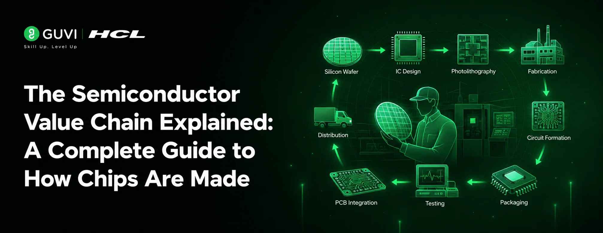
Before looking at each stage in detail, it’s helpful to understand the overall flow. Every semiconductor chip goes through three major stages before it reaches a smartphone, laptop, car, or AI server.
The semiconductor value chain follows a simple sequence:
- Design: Engineers define the chip’s functionality and create its blueprint.
- Manufacturing (Wafer Fabrication): The design is transferred onto silicon wafers inside advanced semiconductor fabrication plants.
- Assembly, Packaging, and Testing (OSAT): The finished silicon dies are packaged, tested, and prepared for use in electronic products.
Although these stages appear straightforward, they are usually handled by different companies. A chip designed in the United States may be manufactured in Taiwan, packaged in Malaysia, and finally assembled into a smartphone in China before being sold globally.
Each stage requires specialized expertise, expensive equipment, and years of technological innovation, which is why the semiconductor industry relies on a global network of companies rather than a single manufacturer.
The sections below explain each stage in detail.
Stage 1: Semiconductor Design (Fabless Companies)
The semiconductor value chain begins with design, the process of creating the blueprint for a chip’s functionality and architecture.
What Happens During Chip Design?
Chip design involves several specialized activities:
Architecture Definition: Engineers define what the chip should do, its performance requirements, power consumption targets, and cost constraints. For example, a mobile processor needs different specifications than a data center accelerator.
Logic Design: Designers create the chip’s logical structure using hardware description languages like Verilog or VHDL. This stage determines how data flows through the chip.
Circuit Design: Engineers translate logical designs into transistor-level circuits, optimizing for speed, power, and area. This is where VLSI design engineers play a crucial role.
Physical Design: Teams create the actual layout of transistors, interconnections, and other components on the silicon die. This involves complex considerations like timing, signal integrity, and manufacturing constraints.
Verification and Validation: Before fabrication begins, designs undergo rigorous testing through simulation to ensure functionality and identify potential issues.
Key Players in Semiconductor Design
The fabless model has become increasingly dominant. NVIDIA, a leading fabless company, captured 7.3% of the global semiconductor market share, driven by explosive demand for AI chips and graphics processors.
Other major fabless companies include:
- Qualcomm: Leading mobile processor and modem designer
- AMD: CPUs and GPUs for computing and gaming
- MediaTek: Mobile and IoT chip solutions
- Broadcom: Networking and communication chips
- Apple: Designs its own processors for iPhones, iPads, and Macs
Tools Used in Chip Design
Chip designers rely on sophisticated Electronic Design Automation (EDA) software:
- Synopsys: Industry leader in EDA tools
- Cadence Design Systems: Comprehensive design and verification tools
- Siemens EDA (formerly Mentor Graphics): PCB and IC design solutions
These tools are essential for managing the complexity of modern chips, which can contain billions of transistors.
Career Opportunities in Chip Design
For VLSI design engineers, this stage offers diverse opportunities:
- Logic Design Engineer: Create digital circuits and systems
- Physical Design Engineer: Handle layout and timing closure
- Verification Engineer: Ensure design correctness through testing
- Analog/Mixed-Signal Designer: Design power management, sensors, and communication circuits
- Architecture Engineer: Define chip specifications and system-level design
Stage 2: Wafer Fabrication (Foundries)
Once a design is complete, it moves to a foundry for wafer fabrication, the most capital-intensive stage of the semiconductor value chain.
What Is Wafer Fabrication?
Wafer fabrication is the process of manufacturing integrated circuits on silicon wafers. This process occurs in highly controlled cleanroom environments where even microscopic dust particles can ruin chips.
A single speck of dust smaller than a human hair can destroy an entire chip during fabrication. That’s why cleanrooms are 10,000 times cleaner than a hospital operating room.
The Fabrication Process:
Wafer Preparation: Pure silicon is melted and grown into crystalline ingots, then sliced into thin wafers. Modern fabs typically use 300mm (12-inch) wafers, with some moving to 450mm.
Photolithography: Circuit patterns are transferred onto wafers using light exposure through masks. This is repeated dozens of times to build up the multiple layers of a chip.
Etching: Chemical processes remove material to create circuit patterns. Advanced etching techniques achieve features smaller than 7 nanometers.
Deposition: Thin films of various materials are deposited onto wafers to create conducting and insulating layers.
Doping: Impurities are introduced into specific regions to modify electrical properties, creating transistors and other components.
Metallization: Metal interconnects are added to link different components on the chip.
Foundry Market Leadership
TSMC dominates the global foundry market with a 64.9% market share in Q3 2024, making it the world’s largest contract chip manufacturer. The company produces chips for Apple, NVIDIA, AMD, and even Intel.
TSMC’s Competitive Advantages:
- Leadership in advanced process nodes (3nm and upcoming 2nm)
- Superior yield rates and manufacturing consistency
- Strong relationships with fabless customers
- Massive production capacity exceeding 17 million 12-inch equivalent wafers annually
Samsung Foundry holds approximately 9-12% market share, making it the second-largest foundry. However, it faces challenges with yield rates at advanced nodes, which has limited its ability to capture more market share.
Other notable foundries:
- GlobalFoundries: Focuses on mature process nodes for automotive and IoT
- SMIC: China’s largest foundry, growing despite U.S. sanctions
- Intel Foundry Services: Intel’s emerging foundry business
Why Foundries Matter?
Foundries represent a critical bottleneck in the semiconductor supply chain. With TSMC manufacturing over 90% of the world’s advanced logic chips below 7nm, any disruption can have cascading effects across the global electronics industry.
This concentration has prompted governments worldwide to invest in domestic manufacturing capabilities:
- U.S. CHIPS Act: $52 billion allocated to strengthen domestic semiconductor manufacturing
- European Chips Act: 43 billion euros committed to boost European semiconductor production
- China’s Investment Fund: $47.5 billion announced in 2024 for chip manufacturing support
Want to understand how governments are strengthening semiconductor manufacturing? Learn how India’s Semiconductor Mission is creating fabs, attracting global investments, and opening thousands of career opportunities for future chip engineers.
Career Opportunities in Fabrication
Careers in foundries focus on manufacturing excellence:
- Process Engineer: Optimize fabrication processes for yield and efficiency
- Equipment Engineer: Maintain and advance manufacturing tools
- Yield Engineer: Analyze and improve production yields
- Integration Engineer: Ensure different process steps work together seamlessly
- Facilities Engineer: Manage cleanroom infrastructure and utilities
Stage 3: Assembly, Testing, and Packaging (OSAT)
The final stage of the semiconductor value chain is OSAT (Outsourced Semiconductor Assembly and Test). This stage transforms fabricated wafers into individual, packaged chips ready for integration into electronic devices.
What Does OSAT Involve?
Wafer Dicing: Wafers containing hundreds or thousands of chips are cut into individual dies using precision sawing or laser cutting.
Die Attachment: Individual dies are mounted onto package substrates using adhesives or solder bumps.
Wire Bonding or Flip-Chip: Electrical connections are made between the die and package. Traditional wire bonding uses thin gold or copper wires, while flip-chip technology places connections directly on the die surface.
Encapsulation: Chips are sealed in protective packages (plastic, ceramic, or metal) to shield them from environmental damage.
Testing: Rigorous electrical testing ensures chips meet specifications. Defective units are identified and removed.
Burn-In: Chips undergo stress testing at elevated temperatures to identify early failures.
The Growing Importance of Advanced Packaging
As Moore’s Law slows, advanced packaging has become crucial for continuing performance improvements. Techniques like 2.5D/3D packaging, chiplets, and heterogeneous integration allow multiple dies to be combined in single packages.
- Apple’s M-series processors use advanced packaging to combine CPU, GPU, and memory in unified packages, improving performance and efficiency.
- AMD’s Ryzen processors leverage chiplet architectures, combining multiple compute dies with I/O dies using advanced packaging techniques.

Major OSAT Players
The OSAT market is dominated by Asian companies:
- ASE Technology Holding (Taiwan): World’s largest OSAT provider
- Amkor Technology (U.S./Asia): Second-largest OSAT with major operations in Asia
- JCET (China): Rapidly growing Chinese OSAT provider
- SPIL (Taiwan): Major packaging and testing specialist
Mainland China and Taiwan together control a significant portion of global OSAT capacity, though countries in Southeast Asia, Eastern Europe, and Latin America are expanding their presence.
Career Opportunities in OSAT
OSAT offers specialized career paths:
- Packaging Engineer: Develop new packaging technologies and processes
- Test Engineer: Design and implement chip testing solutions
- Quality Engineer: Ensure product reliability and quality standards
- Failure Analysis Engineer: Investigate and resolve product failures
- Process Development Engineer: Improve packaging and testing processes
Modern EVs depend heavily on advanced chip packaging and high-performance semiconductors. Explore how VLSI technology powers electric vehicles and enables smarter, safer, and more efficient transportation.
Semiconductor Supply Chain: Global Distribution
The semiconductor supply chain is geographically concentrated, creating both efficiencies and vulnerabilities.
Regional Specialization
United States: Dominates in design, electronic design automation (EDA) tools, and semiconductor equipment manufacturing. Companies like NVIDIA, Qualcomm, AMD, Synopsys, Cadence, and Applied Materials lead their respective segments.
Taiwan: Controls advanced foundry manufacturing through TSMC, which produces over 90% of the world’s advanced logic chips below 7nm.
South Korea: Leads in memory chip production through Samsung and SK Hynix, and maintains strong foundry capabilities.
Japan: Excels in semiconductor materials and specialized equipment. Companies like Tokyo Electron and JSR are critical suppliers.
Europe: Strong in semiconductor equipment (ASML in the Netherlands produces essential lithography machines) and automotive chips (NXP, Infineon).
China: Rapidly expanding across all segments but constrained by U.S. sanctions on advanced technology access.
Supply Chain Vulnerabilities
The semiconductor supply chain has over 50 points where a single region controls more than 65% of global market share, creating significant risks:
- Geopolitical tensions: U.S.-China tech conflicts impact supply chain decisions
- Natural disasters: Taiwan’s earthquake risk threatens TSMC operations
- Pandemic disruptions: COVID-19 exposed supply chain fragility
- Single points of failure: Heavy concentration in specific regions
Diversification Efforts
Governments and companies are actively working to diversify the semiconductor supply chain:
- TSMC is building fabs in Arizona (U.S.), Dresden (Germany), and Kumamoto (Japan)
- Samsung is expanding foundry capacity in Texas
- Intel is investing $33 billion in a fab complex in Germany
- The U.S. is projected to increase wafer fabrication capacity by 203% by 2032
Real-World Example: How Your Smartphone Chip Is Made
Let’s trace the complete semiconductor value chain for a typical smartphone processor, such as the Apple A-series chip.
Stage 1: Design (Apple – Fabless)
- Apple’s engineering team in Cupertino, California, designs the A-series processor architecture.
- They define specifications for CPU performance, GPU capabilities, a neural engine for AI tasks, and power efficiency.
- Using EDA tools from Synopsys and Cadence, they create detailed designs containing billions of transistors.
- This process takes 18-24 months.
Stage 2: Fabrication (TSMC – Foundry)
- Apple sends the completed design files to TSMC in Taiwan.
- TSMC manufactures the chips using its advanced 3nm process technology.
- The fabrication process takes 2-3 months, with wafers passing through hundreds of processing steps in ultra-clean facilities.
- TSMC produces thousands of chips on each 300mm wafer. After fabrication, each wafer contains hundreds of identical processor dies.
Stage 3: Packaging and Testing (OSAT)
- The fabricated wafers move to OSAT facilities, often operated by ASE Technology or other packaging specialists.
- Here, wafers are diced into individual chips, which are then packaged, tested, and prepared for integration.
- Advanced packaging techniques may combine the processor with memory chips using techniques like Package-on-Package (PoP) or through-silicon vias (TSV).
Stage 4: Integration and Assembly
- The packaged chips are shipped to assembly facilities in China or other manufacturing hubs, where they’re integrated into iPhone logic boards alongside other components: memory, power management, wireless modules, and sensors.
Stage 5: End Product
- The finished iPhone reaches consumers worldwide, with the processor representing months of work across multiple continents and dozens of specialized companies.
A single advanced semiconductor fabrication facility costs between $10-20 billion to build, more than some countries’ annual GDP. TSMC’s planned Arizona fab complex represents a $165 billion investment.
Common Mistakes When Understanding the Semiconductor Ecosystem
Mistake 1: Confusing Fabless Companies with Foundries
- Many people assume NVIDIA or Qualcomm manufacture their own chips.
- In reality, these are fabless companies; they design chips but rely on foundries like TSMC for manufacturing.
- Understanding this distinction is crucial for career planning.
Mistake 2: Underestimating the Importance of Packaging
- There’s a misconception that chip design is everything and packaging is trivial.
- In reality, advanced packaging is becoming increasingly critical for performance, power efficiency, and miniaturization.
- The OSAT stage represents significant technical complexity and innovation.
Mistake 3: Ignoring Geopolitical Factors
- The semiconductor supply chain isn’t purely technical; it’s deeply intertwined with geopolitics.
- U.S.-China tensions, Taiwan’s strategic position, and government industrial policies significantly impact the industry.
- Ignoring these factors leads to incomplete understanding.
Mistake 4: Assuming All Chips Use Cutting-Edge Technology
- While cutting-edge chips (3nm, 5nm) get the most attention, the majority of semiconductor production uses mature process nodes (28nm and above).
- Automotive, industrial, and IoT applications often don’t require the most advanced technology.
Mistake 5: Overlooking Career Opportunities Beyond Design
- Many aspiring engineers focus exclusively on chip design roles.
- However, foundries and OSAT providers offer excellent career opportunities in process engineering, test engineering, packaging development, and manufacturing management.
Career Opportunities in the Semiconductor Value Chain
The semiconductor industry offers diverse career paths across all stages of the value chain.
Design-Focused Careers (Fabless Companies)
- VLSI Design Engineer: Design digital and analog circuits
- Verification Engineer: Ensure design correctness
- Physical Design Engineer: Handle layout and timing
- Architecture Engineer: Define chip specifications
- FPGA Engineer: Work with programmable logic devices
Average salaries in India: ₹8-25 lakhs per annum, depending on experience and specialization.
Manufacturing-Focused Careers (Foundries)
- Process Engineer: Optimize fabrication processes
- Equipment Engineer: Maintain manufacturing tools
- Yield Engineer: Improve production yields
- Integration Engineer: Coordinate process steps
- Facilities Engineer: Manage cleanroom infrastructure
Packaging and Testing Careers (OSAT)
- Packaging Engineer: Develop packaging solutions
- Test Engineer: Design testing methodologies
- Quality Engineer: Ensure product reliability
- Failure Analysis Engineer: Investigate defects
How to Start Your Career?
For those aspiring to enter the semiconductor industry, specialized training is essential. The VLSI Design Course from HCL GUVI provides comprehensive training in:
- Digital and analog VLSI design fundamentals
- Verilog/VHDL hardware description languages
- Physical design and verification
- Industry-standard EDA tools
- Hands-on projects with real-world applications
This program is designed to prepare you for roles in fabless companies, foundries, and semiconductor design services.
Conclusion
The semiconductor value chain is a remarkable example of global collaboration and specialized expertise. From fabless companies designing the next generation of AI chips, to foundries fabricating them with atomic precision, to OSAT providers packaging and testing the final products, each stage represents essential contributions to modern technology.
As the world becomes increasingly dependent on semiconductors, from smartphones to AI systems to electric vehicles, professionals who understand this value chain will be in high demand.
The journey begins with knowledge, and this guide provides the foundation for exploring one of the most dynamic and important industries of our time.
Frequently Asked Questions (FAQs)
1. What is the semiconductor value chain?
The semiconductor value chain is the complete sequence of activities from design to manufacturing to packaging that transforms raw silicon into finished microchips. It involves specialized companies handling different stages, including fabless design companies, foundries, and OSAT providers.
2. What is the difference between fabless companies and foundries?
Fabless companies design semiconductor chips but don’t manufacture them. Foundries are manufacturing facilities that produce chips designed by fabless companies. For example, NVIDIA is fabless and designs chips, while TSMC is a foundry that manufactures them.
3. What does OSAT mean in the semiconductor industry?
OSAT stands for Outsourced Semiconductor Assembly and Test. These companies handle the final stages of chip production: dicing wafers, packaging individual chips, and performing electrical testing to ensure quality before chips are integrated into devices.
4. Why is TSMC so important in the semiconductor supply chain?
TSMC (Taiwan Semiconductor Manufacturing Company) controls approximately 64.9% of the global foundry market and manufactures over 90% of the world’s advanced logic chips below 7nm. This makes it a critical node in the global semiconductor ecosystem.
5. What are the main stages of semiconductor manufacturing?
The three main stages are:
(1) Design: Creating chip blueprints using EDA tools,
(2) Wafer Fabrication: Manufacturing circuits on silicon wafers in cleanrooms, and
(3) Assembly and Testing: Packaging individual chips and verifying functionality.
6. Which countries dominate the semiconductor value chain?
Taiwan leads in foundry manufacturing (TSMC), South Korea dominates memory chips (Samsung, SK Hynix), the U.S. leads in design and EDA tools (NVIDIA, Qualcomm, Synopsys), and Japan excels in materials and equipment. China is rapidly expanding across all segments.
7. What career opportunities exist in the semiconductor industry?
Careers span VLSI design engineering, verification engineering, process engineering, packaging engineering, test engineering, and manufacturing management. Opportunities exist in fabless companies, foundries, OSAT providers, and semiconductor equipment companies.
8. How much does it cost to build a semiconductor fabrication facility?
An advanced semiconductor fabrication facility costs between $10-20 billion. This includes ultra-clean manufacturing spaces, sophisticated equipment, and massive infrastructure. TSMC’s planned Arizona investment totals $65 billion.
9. What is the difference between IDM and fabless business models?
IDMs (Integrated Device Manufacturers) like Intel and Samsung handle design, manufacturing, and packaging in-house. Fabless companies like NVIDIA and Qualcomm design chips but outsource manufacturing to foundries, reducing capital requirements.
10. How is the semiconductor supply chain changing?
Governments worldwide are investing in domestic manufacturing to reduce dependency on concentrated regions. The U.S. CHIPS Act, European Chips Act, and similar initiatives are driving geographic diversification. Advanced packaging and chiplet architectures are also reshaping the value chain.
Success Stories

About the Author
Hashmithaa
Hi, I’m Hashmithaa — a content writer with a love for words. Writing isn’t just what I do; it’s how I connect, communicate, and create meaning in a noisy digital world. And if my words help someone make a better decision, learn something new, or feel more confident, then I’ve done my job well.
View all posts by Hashmithaa
Connect with me @








Did you enjoy this article?