


VLSI Design Articles
Why Chips Fail: A Basic Guide to Chip Defects and IC Failure Analysis
Fun Facts About the Semiconductor Industry
Why Are Semiconductor Chips Expensive? Manufacturing Cost Explained
Instruction Set Architecture: How ISA Shapes Modern Chip Design


Get In Touch For Details! Request More Information
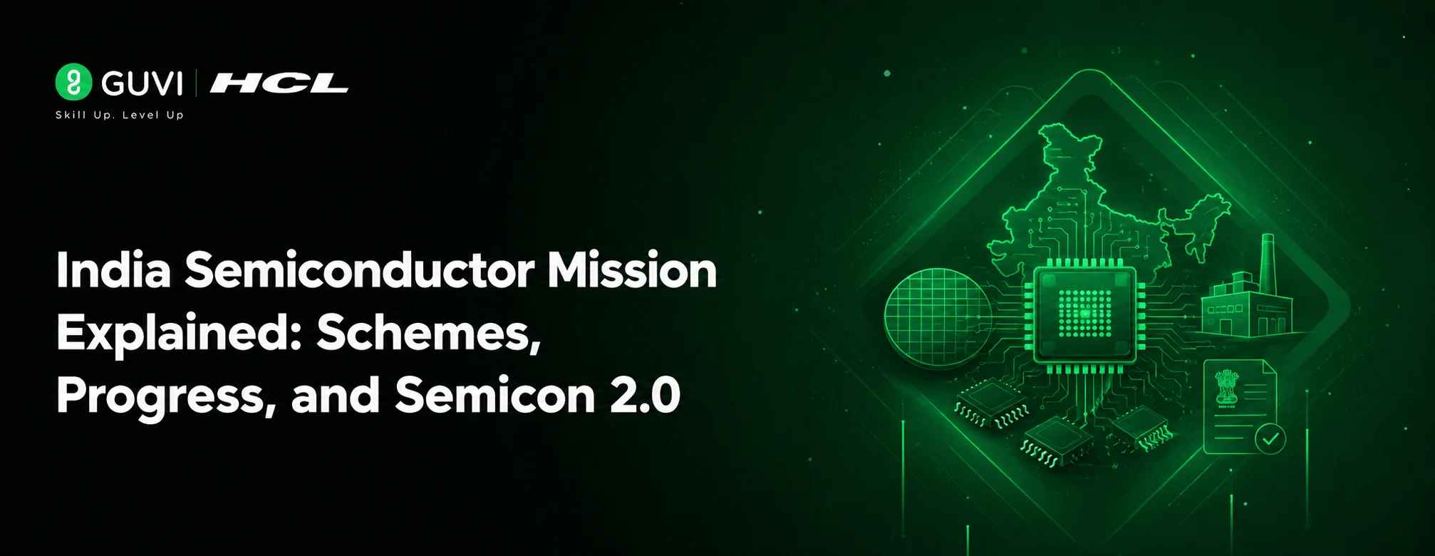
India Semiconductor Mission Explained: Schemes, Progress, and Semicon 2.0 – Best Guide 2026
Jul 28, 2026 10 Min Read 339 Views
(Last Updated)
Table of contents
- TL;DR
- What Is the India Semiconductor Mission?
- What Is the Simple Meaning of the India Semiconductor Mission?
- Why Was the India Semiconductor Mission Launched?
- To Reduce Supply-Chain Risk
- To Move Beyond Electronics Assembly
- To Build Strategic Technology Capability
- To Create High-Skill Employment
- How Has the India Semiconductor Mission Evolved?
- Why Do the ₹1,000 Crore and ₹1,27,500 Crore Figures Both Appear?
- What Are the Main Schemes Under the India Semiconductor Mission?
- Scheme for Semiconductor Fabs
- Scheme for Display Fabs
- Compound Semiconductor and ATMP/OSAT Scheme
- Design Linked Incentive Scheme
- What Are the Six Pillars of Semicon 2.0?
- Design and Indian IP
- Machines, Materials, Chemicals, and Gases
- More Semiconductor Fabs
- Stronger ATMP and OSAT Capability
- Research and Development
- Talent Development
- How Does the India Semiconductor Mission Work?
- Step 1: Define the Project
- Step 2: Evaluate Technical and Financial Feasibility
- Step 3: Coordinate Central and State Support
- Step 4: Approve Incentives Against Milestones
- Step 5: Build and Commission the Capability
- Step 6: Connect Projects to the Wider Ecosystem
- What Progress Has India Made by 2026?
- Manufacturing Projects
- Design and Startup Support
- University and EDA Infrastructure
- Long-Term Market Opportunity
- What Are Some Real Semiconductor Projects in India?
- Tata Electronics Silicon Fab in Dholera
- Micron Assembly and Test Facility in Sanand
- Tata Electronics Packaging Facility in Assam
- Why Does the Mission Matter to India?
- Economic Value
- Supply Resilience
- Technology Ownership
- Support for Major Industries
- Regional Industrial Development
- What Challenges Could Slow the Mission?
- High Capital and Long Payback Periods
- Technology and Equipment Dependence
- Reliable Infrastructure
- Supplier Depth
- Talent Across the Complete Value Chain
- Moving From Approval to Commercial Production
- What Should the Mission Prioritise Next?
- What Does the Mission Mean for Students and Engineers?
- Potential Career Areas
- Skills to Build
- Common Mistakes About India’s Chip Mission
- Assuming It Only Funds Chip Fabs
- Treating Every Approved Project as an Operating Factory
- Confusing Packaging With Wafer Fabrication
- Expecting Immediate Self-Sufficiency
- Focusing Only on Advanced Nanometre Nodes
- Build Practical VLSI Skills With HCL GUVI
- Conclusion
- FAQs
- What does the national semiconductor mission do?
- When was the mission launched?
- What is the budget for Semicon 2.0?
- What are the six pillars of Semicon 2.0?
- How many semiconductor manufacturing units have been approved?
- What does the ISM scheme cover?
- Does the mission support chip-design companies?
- Is semiconductor packaging the same as fabrication?
- Will the mission make India fully self-sufficient in chips?
- How can students prepare for semiconductor careers?
TL;DR
The India Semiconductor Mission is the Government of India’s national programme for building domestic capabilities across chip design, wafer fabrication, compound semiconductors, displays, packaging, testing, equipment, materials, research, and workforce development. Its first phase used a ₹76,000 crore incentive framework to attract projects and support design companies. In July 2026, the Cabinet approved Semicon 2.0 with a total outlay of ₹1,27,500 crore and six pillars covering design, machines and materials, more fabs, advanced packaging, R&D, and talent. The mission aims to reduce strategic dependence while integrating India more deeply into global semiconductor supply chains.
The India Semiconductor Mission is India’s long-term effort to build more of the chip value chain within the country instead of depending almost entirely on imported semiconductors and overseas production capacity.
It supports more than large fabrication plants. The programme also covers chip design, packaging, testing, compound semiconductors, equipment, materials, research, and specialised talent.
Its importance increased further in July 2026, when the Cabinet approved Semicon 2.0 with a total outlay of ₹1,27,500 crore and a broader six-pillar strategy.
This guide explains the mission, its schemes, current progress, real projects, challenges, and career relevance in simple terms.
What Is the India Semiconductor Mission?
The India Semiconductor Mission is the nodal national initiative for developing a sustainable and globally competitive semiconductor and display ecosystem in India.
It operates under the Ministry of Electronics and Information Technology and supports the implementation of the wider Semicon India Programme.
Its responsibilities include evaluating eligible proposals, coordinating with central and state governments, facilitating technology partnerships, and administering approved incentives.
The broader India semiconductor policy combines industrial incentives, design support, research, infrastructure, talent development, international partnerships, and domestic electronics demand.
Understanding how VLSI design turns product requirements into working chips helps explain why the mission supports architecture, RTL design, verification, physical design, and fabrication together.
What Is the Simple Meaning of the India Semiconductor Mission?
In simple terms, the India Semiconductor Mission helps companies and institutions design chips, establish semiconductor factories, package and test chips, develop materials and equipment, conduct research, and train specialized engineers.
Its objective is not to manufacture every chip domestically immediately.
The practical goal is to build a connected ecosystem in areas where India can create strategic capability, commercial value, reliable supply, and globally competitive expertise.
The search phrase semiconductor mission India commonly refers to this national programme and its connected design, manufacturing, packaging, research, and skilling initiatives.
Why Was the India Semiconductor Mission Launched?
India is a major electronics producer and consumer, but much of the semiconductor content used in those products comes from outside the country.
NITI Aayog’s 2026 semiconductor roadmap estimates that imports currently meet around 90–95% of India’s semiconductor consumption, even though professionals based in India account for approximately one-fifth of the global semiconductor design workforce.
This creates a clear gap: India has strong design talent and growing electronics demand, but limited domestic manufacturing, materials, equipment, packaging depth, and Indian-owned semiconductor products.
1. To Reduce Supply-Chain Risk
Different types of semiconductor chips support telecommunications, automobiles, energy systems, healthcare equipment, defence, aerospace, industrial machinery, consumer electronics, and artificial intelligence.
A disruption in semiconductor supply can therefore affect several industries at once.
The India Semiconductor Mission aims to create more trusted and diversified capacity while keeping India connected to international technology and supply networks.
2. To Move Beyond Electronics Assembly
Electronics assembly creates jobs and exports, but a large share of technology value can remain with external chip designers, foundries, equipment suppliers, and intellectual-property owners.
The mission seeks to increase domestic participation in higher-value activities such as architecture, IC design, fabrication, advanced packaging, testing, semiconductor materials, and equipment.
This makes the programme central to India chip manufacturing ambitions and to the wider transition from device assembly towards deeper electronics capability.
3. To Build Strategic Technology Capability
Certain applications need trusted products, long support cycles, secure architectures, and greater control over supply.
These requirements are especially important in defence, space, telecommunications, energy, finance, and critical public infrastructure.
Domestic capability does not remove the need for international partnerships, but it gives India more options when supply chains, export rules, or technologies change.
4. To Create High-Skill Employment
Semiconductor development requires engineers in digital design, verification, analog circuits, physical design, process technology, packaging, testing, equipment, materials, firmware, and applications engineering.
The India Semiconductor Mission therefore connects industrial policy with research, university training, startup development, and workforce creation.
The semiconductor industry India is developing will need both design specialists and professionals who understand cleanrooms, equipment, fabrication processes, packaging, testing, and production quality.
How Has the India Semiconductor Mission Evolved?
The first phase focused on creating initial capability and attracting anchor investments.
On July 15, 2026, the Union Cabinet approved Semicon 2.0 with a total budget outlay of ₹1,27,500 crore to deepen India’s semiconductor design and manufacturing ecosystem.
| Area | ISM 1.0 and Semicon India Programme | Semicon 2.0 |
| Starting point | Approved in December 2021 | Approved by the Cabinet in July 2026 |
| Main objective | Establish initial design, fab, display, and packaging capacity | Deepen and scale the complete semiconductor ecosystem |
| Financial framework | ₹76,000 crore incentive framework | ₹1,27,500 crore total programme outlay |
| Manufacturing focus | Silicon fabs, displays, compound semiconductors, ATMP and OSAT | More fabs and stronger advanced ATMP/OSAT capability |
| Design focus | DLI support and professional EDA access | Indian IP, complete chip designs, systems, and commercial products |
| Supply-chain focus | Attract anchor manufacturing projects | Build equipment, materials, chemicals, gases, and resilient suppliers |
| Research focus | Programme-linked design and manufacturing support | Dedicated collaboration on advanced nodes and technologies |
| Talent focus | C2S, ChipIN, EDA access, and chip-design training | Deeper college training plus fab, cleanroom, construction, and ecosystem skills |
The comparison is based on the original mission framework and the Cabinet-approved six-pillar structure announced in July 2026.
The India Semiconductor Mission has therefore moved from proving that projects can be attracted to building the supplier, research, design, production, and talent systems required for long-term competitiveness.
Why Do the ₹1,000 Crore and ₹1,27,500 Crore Figures Both Appear?
The two funding figures associated with Semicon 2.0 refer to different stages of the programme. The Union Budget provided ₹1,000 crore for ISM 2.0 for FY 2026–27, while the Union Cabinet later approved a total programme outlay of ₹1,27,500 crore on July 15, 2026.
The two figures refer to different things:
- ₹1,000 crore: FY 2026–27 budget provision announced in February
- ₹1,27,500 crore: total outlay approved for Semicon 2.0 in July
This distinction should be included because many February and early-2026 articles still show only the smaller annual provision.
What Are the Main Schemes Under the India Semiconductor Mission?
The first phase of the India Semiconductor Mission used several schemes to cover different parts of the semiconductor and display value chain.
The semiconductor value chain connects chip design, equipment, materials, wafer fabrication, packaging, testing, product integration, and distribution.
1. Scheme for Semiconductor Fabs
This scheme supports eligible projects that manufacture semiconductor wafers in India.
The modified scheme provides fiscal support of up to 50% of eligible project cost on a pari-passu basis for approved applicants.
2. Scheme for Display Fabs
Display fabs manufacture panels used in televisions, monitors, phones, automotive systems, and industrial displays.
The modified scheme provides fiscal support of up to 50% of project cost for approved applicants.
3. Compound Semiconductor and ATMP/OSAT Scheme
This scheme covers:
- Compound semiconductors
- Silicon photonics
- Sensors, including MEMS
- Discrete semiconductors
- Semiconductor ATMP
- Outsourced Semiconductor Assembly and Test facilities
These categories matter because the semiconductor ecosystem India is building includes far more than leading-edge silicon processors.
4. Design Linked Incentive Scheme
The DLI scheme supports Indian semiconductor design companies, startups, and MSMEs through financial assistance, design infrastructure, and product-development support.
By July 2026, 24 design projects had been approved for financial support, while 105 startups and MSMEs had received access to industry-standard EDA tools.
The India Semiconductor Mission uses DLI to convert India’s engineering base into more domestic semiconductor IP, ASICs, SoCs, and market-ready chip products.
A January 2026 PIB update reported that DLI-supported projects had completed 16 chip-design tape-outs, produced six fabricated semiconductor chips, and filed ten patents.
What Are the Six Pillars of Semicon 2.0?
The Cabinet-approved programme defines six pillars for the next phase.
1. Design and Indian IP
The design pillar supports semiconductor IP, complete chip designs, systems, and strategic or commercial products.
The government reported that 105 startups had already started developing chips when Semicon 2.0 was approved.
This pillar gives the India Semiconductor Mission a stronger product-ownership focus instead of limiting policy support to physical manufacturing.
2. Machines, Materials, Chemicals, and Gases
Fabs and packaging plants rely on highly specialised equipment, wafers, chemicals, gases, components, and precision systems.
Semicon 2.0 will incentivise companies working on the manufacturing and R&D of these essential inputs.
The goal is to improve supply resilience and develop precision-manufacturing capability within India.
3. More Semiconductor Fabs
The programme aims to attract additional:
- Silicon fabs
- Compound-semiconductor fabs
- Discrete-component fabs
- Display fabs
India’s first large commercial silicon fab is scheduled for commissioning in 2028, according to the July 2026 Cabinet announcement.
4. Stronger ATMP and OSAT Capability
ATMP and OSAT facilities assemble, package, and test semiconductor dies before they enter electronic products.
Semicon 2.0 aims to attract more advanced packaging technologies rather than treating packaging as a basic final step.
Advanced packaging is also a major part of NITI Aayog’s strategy for making India a top global OSAT and packaging destination.
5. Research and Development
The R&D pillar supports collaboration on advanced process nodes and emerging semiconductor technologies.
It is intended to connect Indian companies and research institutions with leading centres in India and abroad.
NITI Aayog’s roadmap also recommends priorities such as frontier design IP, compound semiconductors, wide-bandgap materials, and advanced packaging.
6. Talent Development
By July 2026, 315 universities were using current EDA tools for complex chip-design training, and approximately 68,000 students had been trained.
The next phase will deepen chip-design education and expand training for cleanrooms, fab construction, process engineering, packaging, and other ecosystem roles.
Together, the six pillars make the India Semiconductor Mission a full-stack industrial programme rather than a single subsidy for chip factories.
The Union Budget initially provided ₹1,000 crore for ISM 2.0 for FY 2026–27. Later, on July 15, 2026, the Union Cabinet approved Semicon 2.0 with a total programme outlay of ₹1,27,500 crore and six strategic pillars. The two figures refer to the annual budget provision and the complete programme outlay, respectively.
How Does the India Semiconductor Mission Work?
A semiconductor proposal must pass through several stages before policy support becomes a functioning industrial capability.
Step 1: Define the Project
A company develops a proposal for a fab, packaging unit, compound-semiconductor facility, display plant, chip-design product, or another eligible activity.
The proposal must explain:
- Technology
- Investment
- Partners
- Location
- Planned capacity
- Implementation schedule
- Commercial case
- Employment
- Utility and infrastructure needs
Step 2: Evaluate Technical and Financial Feasibility
The India Semiconductor Mission evaluates proposals using technical, financial, commercial, strategic, and implementation criteria.
Large projects require credible technology arrangements, long-term funding, suitable land, reliable utilities, supply plans, skilled workers, and customer demand.
Step 3: Coordinate Central and State Support
Semiconductor projects often require central incentives and state-level assistance involving:
- Land
- Electricity
- Water
- Roads and logistics
- Tax support
- Local approvals
- Training infrastructure
The mission works with ministries, state governments, investors, and implementation partners to coordinate these requirements.
Step 4: Approve Incentives Against Milestones
Government support is linked to approved conditions and implementation milestones.
Depending on the project, these may include investment, construction, equipment installation, production, employment, or design-development milestones.
Step 5: Build and Commission the Capability
A manufacturing project must construct facilities, establish cleanrooms, install and qualify equipment, train employees, validate processes, and begin production.
A design project must progress through architecture, RTL, verification, physical implementation, tape-out, fabrication, silicon validation, and product deployment.
These stages form part of the wider semiconductor product lifecycle, which continues from product planning and chip design through manufacturing, validation, deployment, support, and eventual replacement.
Step 6: Connect Projects to the Wider Ecosystem
The long-term value appears when projects buy from local suppliers, train workers, collaborate with universities, serve electronics companies, and create repeat demand.
This is why the India Semiconductor Mission must connect design, production, packaging, suppliers, research, talent, and customers instead of evaluating every factory as an isolated investment.
What Progress Has India Made by 2026?
Manufacturing Projects
By July 2026, 12 semiconductor manufacturing units had been approved with cumulative proposed investment exceeding ₹1.64 lakh crore.
The approved portfolio included:
- One silicon fab
- One silicon-carbide fab
- One integrated gallium-nitride MicroLED display fab
- Nine packaging units
Three companies—Micron, Kaynes, and CG Semi—had started commercial production, while another approved unit was expected to begin during 2026.
Design and Startup Support
Twenty-four semiconductor design projects from startups and MSMEs had been approved for financial support.
Another 105 startups and MSMEs had been granted access to professional EDA tools for products serving satellite communication, drones, surveillance, IoT, LED drivers, AI, telecom, and smart-meter applications.
University and EDA Infrastructure
Professional VLSI design tools are being used across 315 universities.
Government updates also show academic tape-outs through SCL Mohali and overseas foundries, giving students and researchers practical exposure beyond software simulation.
Long-Term Market Opportunity
NITI Aayog’s 2026 roadmap sets an ambition for India to build a USD 120–150 billion domestic semiconductor value chain by 2035.
It organises the broader strategy around five pillars: pioneering innovation, policy and investment, production, people, and partnerships.

The India Semiconductor Mission is one of the main implementation vehicles for turning that national roadmap into projects, intellectual property, infrastructure, suppliers, and skills.
India accounts for nearly one-fifth of the global semiconductor design workforce, while approximately 90–95% of the country’s current semiconductor demand is met through imports. This gap explains why India is working to convert its design talent into deeper product, manufacturing, packaging, and supply-chain capabilities.
What Are Some Real Semiconductor Projects in India?
Tata Electronics Silicon Fab in Dholera
Tata Electronics is establishing a semiconductor fab in Dholera, Gujarat, in technology partnership with Taiwan’s PSMC.
The approved project involves an investment of ₹91,526 crore and planned capacity of approximately 50,000 wafer starts per month.
This project gives the India Semiconductor Mission a major domestic wafer-fabrication anchor for chips serving areas such as automotive, industrial electronics, telecommunications, and consumer devices.
According to the July 2026 Cabinet announcement, India’s first large semiconductor fab is scheduled to be commissioned in 2028.
Micron Assembly and Test Facility in Sanand
Micron’s Sanand facility converts DRAM and NAND wafers from the company’s global manufacturing network into finished memory and storage products through assembly, testing, and packaging.
The approved project involves an investment of ₹22,516 crore and stated production capacity of approximately 14 million units per week.
By July 2026, Micron was among the three approved companies reported to have started commercial production.
The facility demonstrates how packaging and testing can become an early production entry point while India develops wider design, materials, equipment, and fab capability.
Tata Electronics Packaging Facility in Assam
Tata Electronics is establishing a semiconductor packaging facility in Assam with approved investment of ₹27,120 crore.
The project plans to use domestic packaging technologies and has stated capacity of up to 48 million units per day.
These examples show that the India Semiconductor Mission is building different stages of the semiconductor value chain rather than depending on one type of factory.
Why Does the Mission Matter to India?
Economic Value
Semiconductors sit inside electronics products that generate manufacturing output, exports, services, and downstream innovation.
A stronger local ecosystem can retain more value through design, production, packaging, testing, materials, equipment, and product engineering.
Supply Resilience
Domestic capacity cannot remove all global dependencies, and complete semiconductor self-sufficiency is not a realistic near-term goal.
However, more local capability can diversify supply, improve access to selected products, and reduce exposure in strategically important areas.
Technology Ownership
India has deep semiconductor engineering talent, but much of it works on products owned by international companies.
The mission can help create more Indian-owned IP, processors, accelerators, controllers, power devices, and system-level products.
Support for Major Industries
Automobiles, electric mobility, telecommunications, renewable energy, defence, aerospace, healthcare, industrial automation, consumer electronics, and AI infrastructure all need semiconductors.
For example, the role of VLSI in electric vehicles includes battery monitoring, motor control, charging, power conversion, infotainment, connectivity, and safety systems.
The India Semiconductor Mission can support these industries only when chip projects are linked to actual product demand, customer qualification, and dependable production.
Regional Industrial Development
Approved projects are spread across several states and require supporting infrastructure, logistics, suppliers, and training.
This can create specialised industrial clusters rather than isolated factories, although the benefit depends on successful construction, production, and domestic supply linkages.
What Challenges Could Slow the Mission?
The major VLSI design challenges include verification complexity, timing closure, power consumption, high EDA costs, fabrication risks, signal integrity, and long development cycles.
1. High Capital and Long Payback Periods
Semiconductor fabs require very large investments and can take years to construct, qualify, and scale.
Policy support must remain stable across government budgets, market cycles, and technology changes.
2. Technology and Equipment Dependence
Many critical lithography, deposition, inspection, metrology, materials, and EDA technologies are controlled by a limited group of global suppliers.
India needs trusted international partnerships while gradually building selected domestic capabilities.
3. Reliable Infrastructure
Fabs need uninterrupted high-quality electricity, ultra-pure water, specialised gases, waste treatment, logistics, and tightly controlled cleanroom environments.
Announcing a factory is easier than operating it consistently at a competitive yield and cost.
4. Supplier Depth
A functioning semiconductor cluster needs hundreds of suppliers and specialised service providers.
The India Semiconductor Mission must therefore support equipment components, chemicals, gases, wafers, testing, maintenance, precision engineering, and packaging materials—not only final chip plants.
5. Talent Across the Complete Value Chain
India is strong in chip design, but fabs and advanced packaging also need process engineers, material scientists, equipment specialists, cleanroom technicians, yield engineers, construction specialists, and manufacturing managers.
Training capacity must match real project timelines and job roles.
6. Moving From Approval to Commercial Production
Project approval, construction, equipment installation, trial production, qualification, customer acceptance, and profitable scale are separate milestones.
The mission should therefore be judged through operating capacity, yields, design wins, customer orders, patents, exports, employment, and repeat investment—not announcements alone.
What Should the Mission Prioritise Next?
- Execute approved projects on schedule: Construction, equipment qualification, utilities, and production ramp-up need close milestone tracking.
- Support Indian chip products: Design assistance should continue through tape-out, validation, reference boards, software, customer trials, and adoption.
- Develop equipment and material suppliers: Localising selected tools, chemicals, gases, precision parts, and packaging inputs will improve resilience.
- Build advanced-packaging leadership: Chiplets, heterogeneous integration, 2.5D and 3D packaging, and wide-bandgap devices provide opportunities beyond conventional leading-edge fabs.
- Link fabs with domestic demand: Automotive, telecom, energy, defence, industrial, and electronics companies should participate in qualification and long-term procurement.
- Measure results transparently: Reporting should distinguish approvals, construction, installed capacity, production, tape-outs, fabricated chips, jobs, and domestic value addition.
- Maintain global partnerships: India needs international technology, equipment, customers, research, and supply relationships even while strengthening domestic capability.
The India Semiconductor Mission will become more effective when it combines strategic resilience with competitive participation in global supply chains.
What Does the Mission Mean for Students and Engineers?
The programme can expand opportunities across design, manufacturing, packaging, testing, equipment, and materials.
Potential Career Areas
The mission can expand opportunities across several VLSI design job roles, including RTL design, verification, physical design, static timing analysis, DFT, FPGA development, validation, packaging, and semiconductor testing.
- RTL design
- Design verification
- Analog and mixed-signal design
- Physical design
- Static timing analysis
- Design for testability
- FPGA development
- Process engineering
- Equipment engineering
- Packaging and testing
- Product validation
- Semiconductor materials
- Embedded firmware
- Applications engineering
Beginners can follow a step-by-step VLSI roadmap to learn digital electronics, CMOS, Verilog, verification, timing analysis, physical design, scripting, and industry tools in a logical order.
Skills to Build
Building the essential VLSI engineer skills requires electronics fundamentals, HDL programming, verification, scripting, debugging, timing analysis, and practical tool exposure.
Start with:
- Digital electronics
- Boolean logic
- Computer architecture
- MOSFET and CMOS concepts
- Verilog or SystemVerilog
- Linux and scripting
- Functional verification
- Timing fundamentals
- Physical-design basics
- Semiconductor-fabrication overview
- Packaging and testing fundamentals
The India Semiconductor Mission does not guarantee employment by itself.
It creates a wider industrial environment in which learners with strong foundations, practical tool exposure, and demonstrable hardware projects can contribute.
Common Mistakes About India’s Chip Mission
1. Assuming It Only Funds Chip Fabs
The programme also covers design, compound semiconductors, display fabs, packaging, testing, equipment, materials, research, and talent.
Fix: Evaluate the mission across the complete semiconductor value chain.
2. Treating Every Approved Project as an Operating Factory
Approval is an early milestone. Construction, equipment installation, qualification, and commercial production come later.
Fix: Check the current stage of every project before describing it as operational.
3. Confusing Packaging With Wafer Fabrication
ATMP and OSAT facilities package and test fabricated dies. They do not perform the same work as a silicon wafer fab.
Fix: Describe design, fabrication, packaging, testing, and product integration separately.
4. Expecting Immediate Self-Sufficiency
Semiconductor supply chains are globally interconnected and difficult to duplicate fully.
Fix: View the India Semiconductor Mission as a long-term capability-building programme focused on resilience, value creation, and strategic depth.
5. Focusing Only on Advanced Nanometre Nodes
Many automotive, industrial, power, sensor, and communication chips use mature or specialised processes.
Fix: Match process technology to the product’s performance, power, reliability, cost, and production-volume requirements.
Build Practical VLSI Skills With HCL GUVI
India’s semiconductor expansion needs engineers who understand how chip requirements become digital logic, RTL, verified designs, timing-clean implementations, and working hardware.
HCL GUVI’s Certified Professional in VLSI Design and Verification is a six-month live online programme with 180 hours of learning.
Its current curriculum covers digital electronics, MOSFET and CMOS technology, UNIX and scripting, Verilog, static timing analysis, clock-domain crossing, and tools such as Synopsys and Xilinx Vivado.
The programme can help you build practical foundations relevant to India’s growing semiconductor ecosystem. Strengthen the learning with RTL modules, testbenches, FPGA prototypes, timing exercises, and well-documented design projects.
Conclusion
The India Semiconductor Mission has progressed from an initial ₹76,000 crore incentive framework to the Cabinet-approved Semicon 2.0 programme with a total outlay of ₹1,27,500 crore. Its scope now spans design IP, equipment, materials, fabs, advanced packaging, research, and talent. India has approved 12 manufacturing units, supported design startups, expanded EDA access, and started commercial production at selected facilities. The harder phase is execution: completing projects, improving domestic value addition, qualifying products, developing suppliers, and creating sustained customer demand. For learners, strong VLSI, verification, fabrication, and packaging skills can open participation in this expanding ecosystem.
FAQs
1. What does the national semiconductor mission do?
The India Semiconductor Mission supports semiconductor design, manufacturing, packaging, testing, displays, materials, equipment, research, and specialised talent development in India.
2. When was the mission launched?
The first Semicon India Programme was approved in December 2021 with a ₹76,000 crore incentive framework.
Semicon 2.0 was approved by the Union Cabinet on July 15, 2026.
3. What is the budget for Semicon 2.0?
The Cabinet approved Semicon 2.0 with a total outlay of ₹1,27,500 crore.
The earlier ₹1,000 crore figure referred to the FY 2026–27 budget provision announced before the complete programme received Cabinet approval.
4. What are the six pillars of Semicon 2.0?
The six pillars are design and IP, machines and materials, more fabs, stronger ATMP/OSAT capability, research and development, and talent development.
5. How many semiconductor manufacturing units have been approved?
As of July 2026, 12 manufacturing units had been approved with a combined proposed investment exceeding ₹1.64 lakh crore.
6. What does the ISM scheme cover?
The ISM scheme covers silicon fabs, display fabs, compound semiconductors, sensors, discrete semiconductors, ATMP/OSAT, chip design, equipment, materials, research, and workforce development.
7. Does the mission support chip-design companies?
Yes. The DLI scheme supports semiconductor design startups and MSMEs through financial assistance, EDA access, and product-development support.
Twenty-four design projects had been approved for financial support by July 2026.
8. Is semiconductor packaging the same as fabrication?
No. Fabrication creates semiconductor dies on wafers, while ATMP and OSAT facilities assemble, package, and test those dies.
Both are necessary parts of a complete value chain.
9. Will the mission make India fully self-sufficient in chips?
Not immediately. The near-term goal is to build meaningful capability and resilience in selected parts of a globally interconnected industry.
NITI Aayog’s roadmap targets growing levels of domestic capability through 2030 and 2035 rather than immediate isolation from global suppliers.
10. How can students prepare for semiconductor careers?
Students should learn digital electronics, CMOS, Verilog or SystemVerilog, verification, timing, Linux, scripting, fabrication fundamentals, and packaging.
They should also build FPGA and RTL projects that demonstrate practical understanding.
Success Stories

About the Author
Reemsha Khan
Always been a storyteller at heart. Now, I turn complex topics into simple, easy-to-understand stories through content. Hope you find it helpful.
View all posts by Reemsha Khan
Connect with me @








Did you enjoy this article?