


VLSI Design Articles
Why Chips Fail: A Basic Guide to Chip Defects and IC Failure Analysis
Fun Facts About the Semiconductor Industry
Why Are Semiconductor Chips Expensive? Manufacturing Cost Explained
Instruction Set Architecture: How ISA Shapes Modern Chip Design


Get In Touch For Details! Request More Information
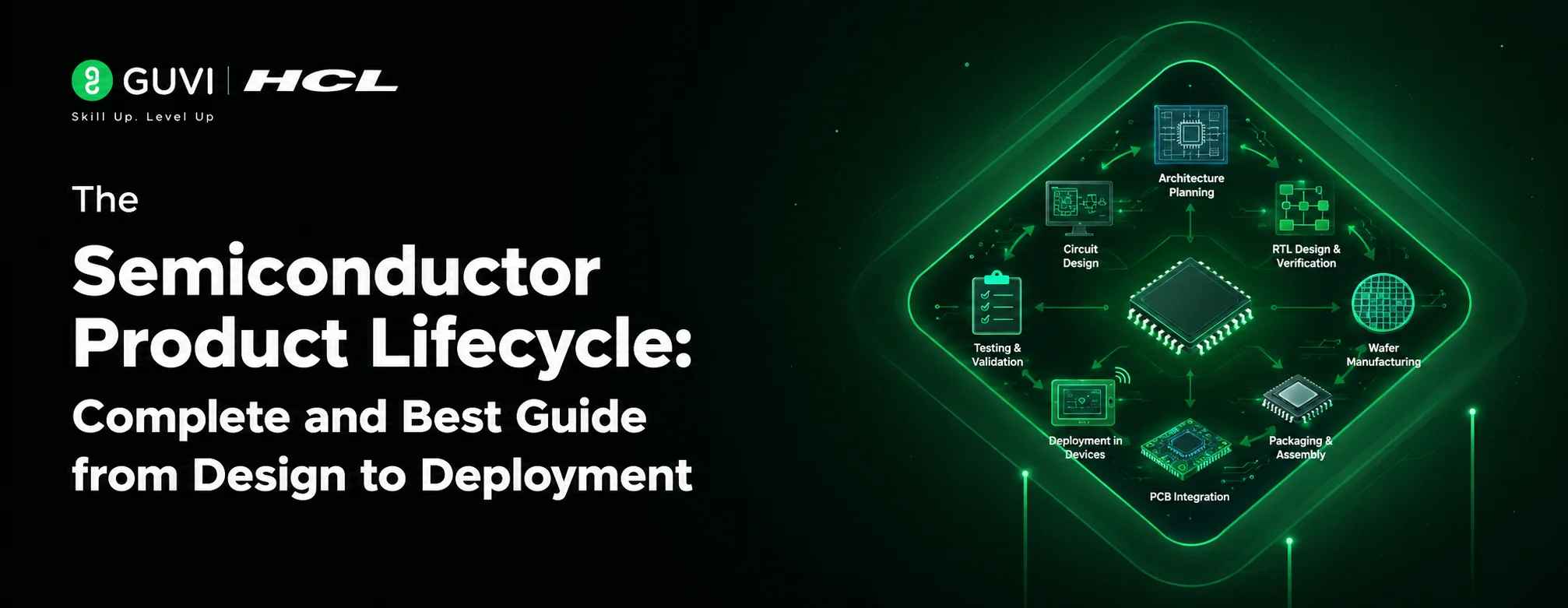
The Semiconductor Product Lifecycle: Complete and Best Guide from Design to Deployment
Jul 21, 2026 7 Min Read 552 Views
(Last Updated)
Table of contents
- TL;DR
- Introduction to Semiconductor Product Development
- What is the Semiconductor Product Lifecycle?
- The Semiconductor Product Lifecycle
- Stage 1: Specification and Architecture Design
- Stage 2: RTL Design and Logic Implementation
- Understanding RTL Design
- Stage 3: Verification and Validation
- Stage 4: Manufacturing and Fabrication
- The IC Manufacturing Process Explained
- From GDSII to Silicon
- Stage 5: Packaging and Assembly
- Stage 6: Testing and Quality Assurance
- Stage 7: Deployment and Lifecycle Management
- Comparison: Traditional vs. Modern Semiconductor Design Flow
- Common Mistakes in Semiconductor Product Development
- Incomplete Specification Analysis
- Underestimating Verification Effort
- Ignoring Power Analysis Until Late
- Poor Clock Domain Crossing Handling
- Neglecting Design for Testability
- Career Opportunities in the Semiconductor Industry
- Growing Demand for VLSI Engineers
- Key Roles in Semiconductor Product Development
- How to Build a Career in VLSI?
- Start Your VLSI Career with GUVI's Zen Program
- Conclusion
- Frequently Asked Questions
- What is the semiconductor product lifecycle?
- How long does the chip development lifecycle typically take?
- What are the main stages of the semiconductor product lifecycle?
- What is RTL in semiconductor design?
- Why is verification important in semiconductor product lifecycle?
- What is the IC manufacturing process?
- What is tape-out in semiconductor development?
- What skills are needed for a career in VLSI design?
- What is Design for Testability (DFT)?
- How can I start a career in semiconductor product development?
TL;DR
- The semiconductor product lifecycle spans six critical stages: specification and design, verification and validation, manufacturing and fabrication, packaging and assembly, testing and quality assurance, and deployment with lifecycle management.
- This process typically takes 18-36 months from concept to mass production.
- Each stage involves specialized engineering teams, advanced tools, and rigorous quality checks.
- For aspiring VLSI engineers, mastering this lifecycle opens doors to roles in chip design, verification, and manufacturing.
Introduction to Semiconductor Product Development
Every electronic device you use today, from smartphones to medical equipment, relies on semiconductor chips. These tiny silicon wafers power modern technology, making the semiconductor product development process one of the most critical engineering workflows in the world.
The journey from an idea to a functioning chip is complex and fascinating. It involves hundreds of engineers working across multiple disciplines, millions of dollars in investment, and cutting-edge technology at every step.
The semiconductor design flow has evolved significantly over the past decades. Earlier, chips contained thousands of transistors; today’s advanced processors pack over 100 billion transistors on a single die. This exponential growth demands sophisticated design methodologies and tools.
For professionals entering this field, understanding the chip development lifecycle is non-negotiable. This guide breaks down each stage of the semiconductor product lifecycle with practical examples, real-world insights, and actionable knowledge you can apply in your career.
What is the Semiconductor Product Lifecycle?
The semiconductor product lifecycle refers to the complete journey of a chip from conception to end-of-life. It covers six distinct stages:
- Specification and Architecture Design
- RTL Design and Logic Implementation
- Verification and Validation
- Manufacturing and Fabrication
- Packaging and Assembly
- Testing and Quality Assurance
- Deployment and Lifecycle Management
Each stage builds upon the previous one. A mistake at any point can cascade into costly failures downstream.
The semiconductor product lifecycle ensures that chips meet performance, power, and area requirements while staying within budget and timeline constraints.
The Semiconductor Product Lifecycle
Stage 1: Specification and Architecture Design
What Happens in the Specification Phase?
The semiconductor product lifecycle begins with defining what the chip must accomplish. This phase determines the entire project’s direction and success.
Product managers and architects collaborate to create detailed specifications. These documents outline performance requirements, power budgets, target applications, area constraints, and cost targets.
A well-defined specification prevents costly changes later in the development cycle. Studies show that fixing a design error in later stages costs 10-100 times more than catching it during specification.
Architecture Design and Planning
Once specifications are finalized, architects create the chip’s high-level structure. This involves:
- Block diagram creation: Breaking down the system into functional blocks
- Interface definition: Establishing communication protocols between blocks
- Power planning: Designing power distribution networks
- Clock architecture: Planning timing and synchronization strategies
Architecture decisions directly impact performance, power consumption, and area (PPA), the three critical metrics in the semiconductor design flow.
Real-World Example: Mobile Processor Architecture
Consider Qualcomm’s Snapdragon processors. Architects must balance performance demands (for gaming and AI) with strict power constraints (for battery life).
The architecture team defines separate processing units: CPU, GPU, DSP, and AI engine, each optimized for specific workloads.
This phase typically lasts 2-4 months for complex chips. Architecture reviews involve stakeholders from design, verification, software, and manufacturing teams to ensure feasibility.
The global semiconductor industry generated $574 billion in revenue in 2024, with projections reaching $1 trillion by 2030. Source: Semiconductor Industry Association
Stage 2: RTL Design and Logic Implementation
Understanding RTL Design
Register Transfer Level (RTL) design transforms architectural specifications into implementable code. Engineers write hardware description language (HDL) code, typically Verilog or VHDL, that defines the chip’s digital logic.
RTL design represents the core of the semiconductor design flow. Designers create functional blocks, state machines, data paths, and control logic based on architecture documents.
The IC manufacturing process depends entirely on accurate RTL code. Even minor errors can render a chip non-functional, making this stage critical.
Key Activities in RTL Design
| Activity | Description | Tools Used |
| Coding | Writing Verilog/VHDL for logic blocks | Vim, Emacs, IDEs |
| Integration | Connecting modules into top-level design | Version control systems |
| Linting | Checking code quality and style | Lint tools, SpyGlass |
| CDC Analysis | Handling clock domain crossings | CDC tools |
Design Methodologies
Modern semiconductor product development uses two primary methodologies:
1. Full-Custom Design: Every transistor is manually designed. Used for analog circuits and high-performance digital blocks requiring optimization.
2. Semi-Custom Design (ASIC Flow): Uses pre-designed standard cells and automated place-and-route tools. Most digital chips follow this approach for efficiency.
Low-Power Design Techniques
Power consumption is a critical concern in modern chips. RTL designers implement various techniques:
- Clock gating: Disabling clocks to inactive blocks
- Power gating: Shutting off power to unused sections
- Multi-voltage domains: Operating different blocks at optimal voltages
- Dynamic voltage frequency scaling (DVFS): Adjusting voltage and frequency based on workload
Modern mobile processors use over 20 different power domains to optimize battery life, with some blocks consuming just microwatts during standby.
Stage 3: Verification and Validation
Why Verification Matters
Verification ensures the chip functions correctly before manufacturing begins. This stage consumes 60-70% of the total design effort in modern semiconductor design flow.
A single bug in a complex chip can cost millions in re-spins. The infamous Intel FDIV bug in 1994 cost the company $475 million in recalls, a lesson that transformed industry verification practices.
Types of Verification
Functional Verification: Confirms the design meets specifications. Includes:
- Simulation-based verification
- Formal verification methods
- Hardware emulation
- FPGA prototyping
Timing Verification: Ensures signals meet setup and hold times across all conditions.
Physical Verification: Checks design rules, connectivity, and manufacturability.
Verification Methodologies
The Universal Verification Methodology (UVM) has become the industry standard. Verification engineers create:
- Testbenches that stimulate the design
- Checkers that validate responses
- Coverage models that track verification completeness
Code Coverage and Functional Coverage
Coverage metrics quantify verification progress:
| Coverage Type | What It Measures | Target |
| Code Coverage | Lines, branches, conditions executed | 100% |
| Functional Coverage | Features and scenarios tested | 95% |
| Assertion Coverage | Properties checked | 100% |
Emulation and Prototyping
For complex chips, software simulation is too slow. Teams use:
- Hardware emulators: Specialized systems that run designs at near-real speeds
- FPGA prototypes: Mapping designs to FPGAs for software development
These platforms enable early software development, saving months in overall chip development lifecycle.
Stage 4: Manufacturing and Fabrication
The IC Manufacturing Process Explained
Once verification passes, the design moves to fabrication. This stage transforms RTL code into physical silicon through a sophisticated process.
The chip development lifecycle reaches its most capital-intensive phase here. A modern fabrication facility (fab) costs $10–20 billion to build.
From GDSII to Silicon
The design data (GDSII format) undergoes several transformations:
1. Mask Creation: Photomasks are created for each layer of the chip. A modern processor may require 60-80 masks.
2. Wafer Preparation: Silicon wafers (typically 300mm diameter) are prepared with crystalline perfection.
3. Photolithography: Patterns are transferred to wafers using light exposure through masks. EUV (Extreme Ultraviolet) lithography enables features below 7nm.
4. Etching and Deposition: Material is selectively removed and added to build transistor structures.
5. Ion Implantation: Dopants are introduced to create transistor regions.
Wafer Fabrication Steps
| Step | Process | Purpose |
| 1 | Cleaning | Remove Contaminants |
| 2 | Oxidation | Grow insulating layers |
| 3 | Photoresist coating | Apply light-sensitive material |
| 4 | Exposure | Transfer pattern through mask |
| 5 | Development | Remove exposed resist |
| 6 | Etching | Remove material selectivity |
| 7 | Doping | Introduce impurities (boron, phosphorus, arsenic) to modify electrical properties |
| 8 | Metal Deposition | Create electrical interconnections between transistors |
This cycle repeats for each layer, taking 8-12 weeks for a complete wafer.
Advanced Manufacturing Technologies
Modern fabs use cutting-edge techniques:
- FinFET transistors: 3D transistor structures for better control
- Gate-All-Around (GAA): Next-generation transistor architecture
- 3D NAND: Stacked memory cells for storage
- Chiplets: Multiple dies in one package
TSMC’s 3nm process can fit approximately 300 million transistors per square millimeter, roughly 100 times denser than a decade ago.
Stage 5: Packaging and Assembly
Why Packaging Matters
Packaging protects the delicate silicon die and provides electrical connections to the outside world. It significantly impacts performance, power, and reliability.
The semiconductor product lifecycle increasingly focuses on advanced packaging as Moore’s Law scaling slows. Modern packages enable heterogeneous integration, combining different chip types in one package.
Types of Packages
Traditional Packages:
- QFP (Quad Flat Package): Leads on all four sides
- BGA (Ball Grid Array): Solder balls underneath
- QFN (Quad Flat No-leads): Compact, exposed pad for heat dissipation
Advanced Packages:
- SiP (System-in-Package): Multiple chips in one package
- 2.5D/3D Packaging:Stacked dies with vertical connections
- Fan-Out Wafer-Level Packaging: Direct redistribution on wafer
Packaging Process Flow
- Wafer Dicing: Separating individual dies using precision saws
- Die Attach: Mounting dies to substrate or leadframe
- Wire Bonding/Flip-Chip: Creating electrical connections
- Encapsulation: Molding plastic around the assembly
- Marking and Testing: Final checks before shipment
Thermal and Electrical Considerations
Packaging engineers must address:
- Thermal resistance: Heat dissipation from die to environment
- Electrical parasitics: Inductance and capacitance of interconnects
- Signal integrity: Maintaining signal quality at high speeds
- Mechanical reliability: Surviving thermal cycles and mechanical stress

Stage 6: Testing and Quality Assurance
Semiconductor Testing Overview
Testing ensures only functional chips reach customers. The chip development lifecycle includes multiple testing stages to catch defects early.
Defects occur during manufacturing due to particle contamination, process variations, and equipment issues. Testing identifies and screens these failures.
Types of Tests
Wafer Testing (Probe Testing):
- Tests each die before packaging
- Identifies non-functional chips, saving packaging costs
- Uses probe cards with thousands of tiny needles
Final Testing (Package Testing):
- Tests packaged chips under operating conditions
- Verifies functionality, performance, and reliability
- Includes burn-in testing to weed out early failures
System-Level Testing:
- Tests chips in actual application environments
- Validates software-hardware interaction
- Catches corner cases missed by functional tests
Test Methods
| Test Type | Purpose | Equipment |
| DC Testing | Verify voltage/current levels | ATE (Automated Test Equipment) |
| Functional Testing | Check logical operation | ATE with pattern generators |
| AC Testing | Measure timing parameters | High-speed ATE |
| Memory Testing | Detect bit failures | Memory BIST |
| Boundary Scan | Test interconnects | JTAG |
Yield Optimization
Manufacturing yield, the percentage of good dies is critical for profitability. A 1% yield improvement can save millions in high-volume production.
Yield optimization involves:
- Design for Testability (DFT): Built-in test structures
- Failure Analysis: Root cause investigation of failures
- Process Control: Monitoring and adjusting manufacturing parameters
Modern high-end processors have manufacturing yields of 60-80%, meaning 20-40% of chips are discarded. This is why leading-edge chips are expensive.
Stage 7: Deployment and Lifecycle Management
Product Introduction and Ramp
After testing, chips enter mass production and deployment. This phase requires coordination between design, manufacturing, and customers.
The semiconductor product development cycle concludes with production ramp, gradually increasing manufacturing volume while maintaining quality.
Qualification and Reliability
Before mass deployment, chips undergo rigorous qualification:
- Temperature cycling: Testing across -40°C to +125°C
- Humidity testing: Exposure to moist environments
- ESD testing: Electrostatic discharge resilience
- Life testing: Accelerated aging to predict lifespan
Supply Chain Management
Semiconductor supply chains are complex and global. Key considerations include:
- Capacity planning: Ensuring sufficient fab capacity
- Inventory management: Balancing stock levels and demand
- Geographic risks: Managing concentration in Taiwan, Korea, and the US
End-of-Life Management
Chips eventually reach end-of-life due to:
- Technology obsolescence
- Fab closure for older nodes
- Market demand shifts
Companies must manage product transitions, providing last-time-buy notices and supporting legacy customers.
Comparison: Traditional vs. Modern Semiconductor Design Flow
| Aspect | Traditional Flow | Modern Flow |
| Design Entry | Schematic capture | HLS+RTL |
| Verification | Manual test vectors | UVM+Formal |
| Implementation | Hand place-and-route | Automated flows |
| Sign-off | Corner-based | Statistical (MMM-C) |
| Prototyping | Physical samples | Virtual prototypes |
| Cycle Time | 24-36 months | 12-18 months |
| Team Size | 50-100 engineers | 100-500 engineers |
Modern semiconductor design flow emphasizes parallel activities, automation, and early validation to reduce time-to-market.
Common Mistakes in Semiconductor Product Development
Avoiding these mistakes can save your project millions of dollars and months of delay:
1. Incomplete Specification Analysis
Many projects start with vague requirements. This leads to scope creep, design changes, and schedule slips.
Solution: Spend adequate time on specification. Involve all stakeholders. Document everything clearly.
2. Underestimating Verification Effort
Teams often allocate insufficient resources for verification. This results in bugs escaping to silicon.
Solution: Plan verification from day one. Allocate 60% of effort to verification. Use coverage-driven methodology.
3. Ignoring Power Analysis Until Late
Power problems discovered late are expensive to fix. Thermal issues can require complete redesigns.
Solution: Perform power analysis throughout the design. Use UPF/CPF for power intent. Design for low power from the start.
4. Poor Clock Domain Crossing Handling
CDC bugs are notoriously difficult to find. They cause intermittent failures in production.
Solution: Use CDC analysis tools. Follow strict coding guidelines. Verify CDC paths thoroughly.
5. Neglecting Design for Testability
Chips without proper DFT structures are difficult and expensive to test.
Solution: Integrate scan chains, BIST, and boundary scan. Plan test strategy during architecture phase.
Career Opportunities in the Semiconductor Industry
Growing Demand for VLSI Engineers
The semiconductor industry faces a significant talent shortage. India alone will need 1 million semiconductor professionals by 2030, according to the India Semiconductor Mission.
Key Roles in Semiconductor Product Development
| Role | Responsibilities | Skills Required |
| Design Engineer | RTL coding, architecture | Verilog, SystemVerilog, digital design |
| Verification Engineer | Testbench development, simulation | UVM, SystemVerilog, scripting |
| Physical Design Engineer | Place-and-route, timing closure | CAD tools, timing analysis |
| DFT Engineer | Test structure insertion | Scan, BIST, ATPG |
| Design Verification Engineer | Formal Verification | Formal tools, property checking |
| Application Engineer | Customer Support | Technical communication, debugging |
How to Build a Career in VLSI?
Step 1: Build strong fundamentals in digital electronics and computer architecture.
Step 2: Learn hardware description languages (Verilog, SystemVerilog, VHDL).
Step 3: Master verification methodologies (UVM, formal verification).
Step 4: Gain hands-on experience with industry tools through projects.
Step 5: Apply for internships and entry-level positions at semiconductor companies.
Start Your VLSI Career with GUVI’s Zen Program
If you’re serious about building a career in the semiconductor industry, structured learning accelerates your journey significantly.
HCL GUVI’s VLSI Design Course covers the complete semiconductor product lifecycle from RTL design to verification and physical design. You’ll work on industry-relevant projects using professional tools, gaining practical skills that employers seek.
The program includes:
- Comprehensive curriculum covering design, verification, and physical design
- Hands-on projects with real-world complexity
- Mentorship from industry experts
- Placement assistance with top semiconductor companies
Whether you’re a fresh graduate or a working professional looking to switch domains, this program provides the structured path you need.
Conclusion
The semiconductor product lifecycle represents one of engineering’s most sophisticated workflows. From initial specification to final deployment, each stage requires specialized knowledge, tools, and collaboration.
Understanding this lifecycle is essential for anyone pursuing a career in chip development. The semiconductor design flow continues to evolve, with new methodologies and technologies emerging regularly.
For aspiring engineers, mastering these concepts opens doors to exciting opportunities in a growing industry. The demand for skilled VLSI professionals will only increase as chips become more central to technology.
Frequently Asked Questions
1. What is the semiconductor product lifecycle?
The semiconductor product lifecycle is the complete journey of a chip from concept to deployment, including specification, design, verification, manufacturing, packaging, testing, and lifecycle management.
2. How long does the chip development lifecycle typically take?
The chip development lifecycle typically takes 18-36 months for complex chips, depending on complexity, technology node, and team experience.
3. What are the main stages of the semiconductor product lifecycle?
The main stages include specification, architecture design, RTL design, verification, synthesis, physical design, manufacturing, packaging, and testing.
4. What is RTL in semiconductor design?
RTL (Register Transfer Level) is a design abstraction where digital circuits are described using hardware description languages like Verilog or VHDL, defining data flow and control logic.
5. Why is verification important in semiconductor product lifecycle?
Verification ensures the chip functions correctly before manufacturing, preventing costly re-spins. It typically consumes 60-70% of the total design effort.
6. What is the IC manufacturing process?
The IC manufacturing process transforms design data into physical silicon through photolithography, etching, deposition, and doping on silicon wafers in specialized fabrication facilities.
7. What is tape-out in semiconductor development?
Tape-out is the milestone when the final design database is sent to the fab for manufacturing. It marks the transition from design to production.
8. What skills are needed for a career in VLSI design?
Key skills include digital design, Verilog/SystemVerilog, verification methodologies (UVM), computer architecture, and familiarity with EDA tools.
9. What is Design for Testability (DFT)?
DFT involves adding special structures to chips that enable efficient testing, including scan chains, built-in self-test (BIST), and boundary scan.
10. How can I start a career in semiconductor product development?
Start by building strong fundamentals in digital electronics, learn HDL languages, take specialized courses like GUVI’s VLSI Design Course, and work on hands-on projects.
Success Stories

About the Author
Hashmithaa
Hi, I’m Hashmithaa — a content writer with a love for words. Writing isn’t just what I do; it’s how I connect, communicate, and create meaning in a noisy digital world. And if my words help someone make a better decision, learn something new, or feel more confident, then I’ve done my job well.
View all posts by Hashmithaa
Connect with me @












Did you enjoy this article?