


VLSI Design Articles
Why Chips Fail: A Basic Guide to Chip Defects and IC Failure Analysis
Fun Facts About the Semiconductor Industry
Why Are Semiconductor Chips Expensive? Manufacturing Cost Explained
Instruction Set Architecture: How ISA Shapes Modern Chip Design

Get In Touch For Details! Request More Information
Top VLSI Design Tools in 2026: Best EDA Software for Students & VLSI Engineers
Sep 08, 2026 11 Min Read 36283 Views
(Last Updated)
TL;DR
- VLSI design tools are Electronic Design Automation (EDA) software used to design, simulate, synthesize, verify, place, route, and sign off integrated circuits.
- The leading VLSI tools in 2026 include Synopsys, Cadence, Siemens EDA, and open-source platforms such as OpenROAD, with AI increasingly integrated into chip-design and verification workflows.
Modern VLSI design just needs sophisticated software tools, whether you’re working on a simple microcontroller or a complex processor. Manual design has become practically impossible because integrated circuits now pack billions of transistors.
Electronic Design Automation (EDA) tools drive successful VLSI design at every step. Your project’s journey from original concept to final tape-out requires VLSI design tools and IC design software to handle chip development effectively.
This complete guide breaks down the best VLSI Design tools available in 2026 and helps you pick the right tools that match your design needs.
Table of contents
- What is VLSI Design?
- What Are VLSI Design Tools?
- Top VLSI Design Tools in 2026and Their Usages
- Essential EDA Tool Suites for Modern Chip Design
- RTL Design and Synthesis Tools
- Physical Design and Layout Tools
- Verification and Testing Tools
- Siemens Questa
- Which VLSI Design Tools Should Indian Students Learn?
- Concluding Thoughts…
- FAQs
- What are the essential software VLSI design tools in 2026?
- How has artificial intelligence impacted VLSI design tools?
- What are the key components of a modern VLSI design workflow?
- How do cloud-based EDA solutions benefit chip designers?
- What are the differences between commercial and open-source EDA tools for VLSI design?
- Which VLSI design tools is best for beginners?
- Which software is used for VLSI physical design?
- Which tools are used for VLSI verification?
- Which software is used for VLSI layout design?
- Is Cadence or Synopsys better for VLSI?
- Which VLSI design tools should I learn for a job in India?
What is VLSI Design?
VLSI (Very Large Scale Integration) design creates integrated circuits by combining millions or billions of transistors onto a single semiconductor chip. Your trip into VLSI design starts with this fundamental technology that revolutionized modern electronics since the 1970s.
What Are VLSI Design Tools?
VLSI design tools are specialized EDA software platforms used to design, simulate, synthesize, implement, verify, and sign off integrated circuits containing millions or billions of transistors.
They automate complex chip-design tasks that would be extremely difficult to perform manually.
VLSI design is a complex process that covers several significant stages. The design flow has:
- System specification and architectural design
- RTL (Register Transfer Level) design
- Functional verification
- Logic synthesis
- Physical design and verification
- Sign-off and fabrication
VLSI design’s evolution tells an impressive story. The original integrated circuits had just a few transistors. Modern microprocessors pack billions of transistors on a single chip. This shows semiconductor technology’s remarkable progress.
Hardware Description Languages (HDLs) like Verilog and VHDL form the backbone of the design process. These languages help you describe and verify digital circuit behavior before physical fabrication.
The process uses specialized Electronic Design Automation (EDA) tools from companies like Cadence, Synopsys, and Mentor Graphics for simulation and verification.
VLSI Design Flow: Where Are These VLSI Design Tools Used?
Before choosing a tool, it helps to understand where it fits in the overall VLSI flow.
| VLSI Design Stage | Main Activity | Popular Tools |
| RTL Design | Write hardware description | Verilog, SystemVerilog, VHDL |
| Simulation | Verify RTL behavior | Synopsys VCS, Siemens Questa, Cadence Xcelium |
| Synthesis | Convert RTL to gate-level netlist | Synopsys Design Compiler, Cadence Genus |
| Floorplanning | Define physical chip structure | Cadence Innovus, Synopsys Fusion Compiler |
| Placement | Position standard cells | Innovus, Fusion Compiler |
| Clock Tree Synthesis | Build clock network | Innovus, Fusion Compiler |
| Routing | Connect design components | Innovus, Fusion Compiler |
| Timing Analysis | Check timing constraints | PrimeTime, Cadence Tempus |
| Power Analysis | Analyze power and integrity | Cadence Voltus, Synopsys PrimePower |
| Physical Verification | DRC/LVS and sign-off | Siemens Calibre, Cadence Pegasus |
| Custom Layout | Analog/mixed-signal layout | Cadence Virtuoso |
| Open-Source RTL-to-GDS | Automated implementation | OpenROAD |
Top VLSI Design Tools in 2026 and Their Usages
VLSI (Very Large Scale Integration) design involves integrating millions of transistors onto a single chip and requires sophisticated tools for various stages of the design process. Below are the essential VLSI design tools, categorized by their roles:
1. Essential EDA Tool Suites for Modern Chip Design
EDA (Electronic Design Automation) in VLSI design refers to a suite of software tools used to design, simulate, verify, and implement complex integrated circuits and semiconductor devices.
These tools automate key processes such as schematic capture, layout design, synthesis, verification, and testing, significantly reducing the time and effort required in chip development.
Modern EDA platforms are also increasingly incorporating AI and automation. Synopsys, Cadence, and Siemens EDA are all expanding AI-driven capabilities across chip design and verification workflows in 2026.
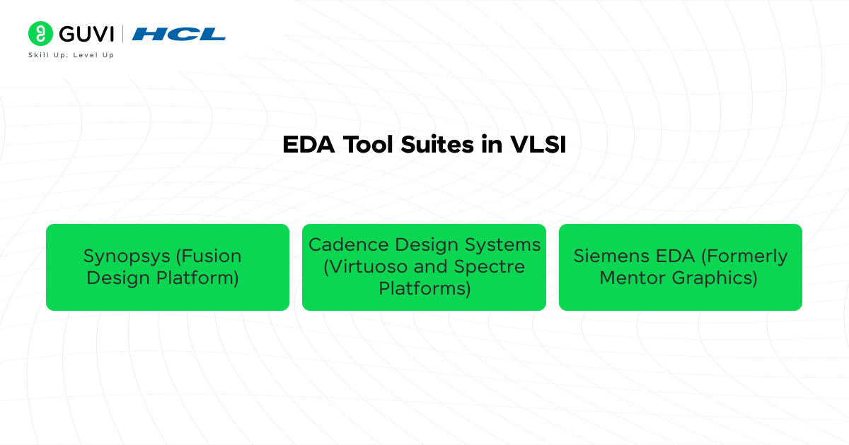
A) Industry-leading Commercial EDA Suites (Synopsys, Cadence, Mentor)
Three major players dominate the EDA software market and reshape the scene of VLSI design tools. Synopsys leads with a midpoint of $9.665 billion in revenue, while Cadence Design Systems generates a midpoint of $6.30 billion, and Siemens EDA (formerly Mentor Graphics) brings in ~$2.1 billion to $2.3 billion. Let’s take a look at them in detail:
1. Synopsys (Fusion Design Platform)
Synopsys is a pioneer in the EDA industry, providing end-to-end solutions for chip design and verification. The Fusion Design Platform integrates cutting-edge tools to deliver optimal Performance, Power, and Area (PPA) metrics.
Its current digital design portfolio includes tools such as Design Compiler NXT, Fusion Compiler, IC Compiler II, VCS, PrimeTime, and DSO.ai.
Key Features:
- Design Compiler: This tool performs advanced RTL synthesis and supports complex power optimizations. It also provides ECO (Engineering Change Order) capabilities for quick design fixes.
- IC Compiler II: It offers concurrent optimization of placement, routing, and clock tree synthesis and is also optimized for advanced nodes (3nm, 5nm).
- PrimeTime: It is an industry-standard tool for static timing analysis (STA) that provides multi-corner, multi-mode (MCMM) analysis.
- VCS: High-performance logic simulation with support for SystemVerilog and UVM. Also includes features like constrained random testing and functional coverage.
- DSO.ai: DSO.ai brings AI-driven design-space exploration into the EDA workflow. Synopsys has also expanded AI capabilities within the Fusion Compiler, enabling adaptive design flows to optimize power, performance, and area (PPA).
2. Cadence Design Systems
Cadence excels in analog, mixed-signal, and digital design environments. The Virtuoso platform is widely used for custom IC design, and the Spectre suite provides precise circuit simulation capabilities.
Its current portfolio includes Virtuoso, Spectre, Genus, Innovus, Tempus, Xcelium, Voltus, Pegasus, and Cerebrus.
Key Features:
- Virtuoso Platform: This platform offers a unified environment for schematic capture, layout editing, and verification. It offers advanced node support with design-rule-driven layout techniques.
- Spectre Simulation Suite: This suite includes Spectre X for high-speed simulation of large-scale designs and provides robust transient, AC, and DC analysis.
- Genus Synthesis Solution: Genus converts RTL into gate-level implementations while optimizing for Power, Performance, Area and Timing.
- Innovus: Innovus is a digital physical implementation tool used for Floorplanning, Placement, Clock-tree synthesis, Routing, Timing optimization and Power optimization.
- Cerebrus: Cerebrus is Cadence’s AI-driven design optimization technology. It helps automate design-space exploration and optimization across implementation workflows.
Cadence continues to enhance Genus for advanced digital and AI-silicon workflows. In 2026, Cadence announced enhancements to Genus and Innovus for next-generation AI silicon and advanced process technologies.
3. Siemens EDA (Formerly Mentor Graphics)
Siemens EDA focuses on multidisciplinary collaboration for chip, PCB, and embedded software designs. Its tools cater to industries such as automotive and aerospace.
Key Features:
- Questa: Questa is used for HDL simulation, Functional verification, Debugging, Coverage analysis, SystemVerilog verification and UVM-based verification. Siemens is also expanding Questa with AI-assisted and agentic verification workflows in 2026.
- Calibre: Calibre is a major physical-verification platform used for Design Rule Checking (DRC), Layout Versus Schematic (LVS), Physical verification, Reliability verification and Advanced-node verification.
- Aprisa: Aprisa is used for digital physical implementation, including placement, routing, and optimization.
- Tessent: Tessent is used for design-for-test (DFT), including test architecture and manufacturing-test workflows.
Siemens’ 2026 AI strategy connects technologies such as Questa, Aprisa, Calibre, Tessent, and Solido with its Fuse EDA AI System to automate workflows across the semiconductor design lifecycle.
B) Popular Open-source EDA Alternatives
Open-source tools offer economical solutions and we have a long way to go, but we can build on this progress.
The OpenROAD project, backed by DARPA and Google, provides a complete toolkit from high-level synthesis to layout generation. Let’s look at it in detail:
1. OpenROAD Project
The OpenROAD Project is an open-source initiative to democratize chip design by providing a fully automated EDA toolchain.
It covers the entire flow from RTL to GDSII, enabling rapid design iterations and accessibility for academia, startups, and smaller enterprises.
Key Features:
- Fully Automated Design Flow:
Automates critical steps such as placement, routing, timing optimization, and clock tree synthesis. Ensures DRC compliance and reduces manual intervention in the design process. - Cloud-Native Architecture:
- Designed for scalability and distributed processing on cloud platforms.
- Offers resource efficiency and cost-effectiveness, making high-performance design accessible.
- Community and Industry Support:
- Actively developed and maintained by leading academic institutions and corporate sponsors.
- A collaborative open-source ecosystem drives regular updates and improvements.
- Customizable Modular Design:
- Flexible modules can be used independently or as part of a complete flow.
- Adaptable to integrate with proprietary tools or workflows for hybrid use cases.
- AI and ML Integration:
Incorporates machine learning techniques for advanced optimization of placement, routing, and power management, improving design quality and efficiency. - Wide Format and Node Compatibility:
- Supports industry-standard design formats such as LEF/DEF, Verilog, and SPEF.
- While primarily targeting mainstream nodes, it extends support to advanced technologies with ongoing updates.
C) Cloud-based EDA Solutions
Cloud computing has altered the map of how you can access and use EDA tools. Let’s look at the top tools in this section:
1. Synopsys Cloud
Synopsys Cloud is a game-changing solution in the EDA space, offering a flexible, pay-per-use model that provides access to the full range of Synopsys tools.
By eliminating the need for significant upfront infrastructure investment, it enables businesses of all sizes to innovate efficiently.
Key Features
- Automatic Workload Distribution:
Synopsys Cloud dynamically allocates workloads between cloud and local environments, optimizing resource usage and performance for complex designs. - Faster Time-to-Market:
Accelerates design cycles by supporting faster iterations and allowing teams to scale resources on demand during critical phases. - Enhanced IP Security:
Employs robust encryption and access control measures to ensure sensitive intellectual property remains secure throughout the cloud workflow.
2. Cadence Managed Cloud Service
Cadence Managed Cloud Service simplifies access to an integrated design and verification environment by offering a pre-configured cloud setup.
This service is tailored to meet the growing demand for hybrid workflows, combining on-premises and cloud solutions seamlessly.
Key Features:
- Pre-configured Cloud Environments:
Provides out-of-the-box configurations with Cadence tools, reducing setup time and ensuring compatibility with the latest design and verification solutions. - Hybrid Workflow Support:
Enables flexible operations by allowing users to integrate on-premises workflows with cloud-based processes, making it ideal for distributed teams. - Secure Global Collaboration:
Facilitates teamwork across geographies with secure data sharing, centralized management, and compliance with global security standards.
2. RTL Design and Synthesis Tools
RTL (Register Transfer Level) design in VLSI focuses on describing a digital circuit’s behavior using hardware description languages (HDLs) like Verilog or VHDL.
It represents the flow of data between registers and the operations performed at each clock cycle.
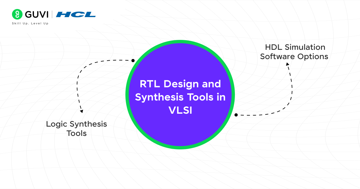
Synthesis converts the RTL code into a gate-level netlist, mapping the design to specific logic gates and flip-flops. This process optimizes the design for timing, area, and power constraints, bridging the gap between high-level functional design and physical implementation.
Your VLSI design success depends on picking the right RTL design and synthesis tools. Let’s look at the software options that make your chip design process smoother.
A) HDL Simulation Software Options
Several powerful options can meet your HDL simulation needs. Let’s look at them in detail:
1. ModelSim
ModelSim has historically been widely used for HDL simulation. In current Siemens EDA workflows, Questa is the more relevant platform to highlight for modern verification.
Its mixed-language capabilities allow seamless simulation of VHDL, Verilog, and SystemVerilog code, making it a favorite among engineers working on diverse projects.
Key Features:
- Mixed-Language Support: Enables simulation of designs written in multiple HDLs within the same project, streamlining workflows.
- Advanced Debugging Tools:
- Waveform viewer for visualizing signal interactions and transitions.
- Breakpoints for step-by-step execution.
- Assertions for identifying logical errors in real-time.
- Integration with FPGA and ASIC Flows: Ensures compatibility with industry-standard tools for seamless handoffs.
2. Xilinx Vivado Simulator (XSIM)
The Xilinx Vivado Simulator (XSIM) is a high-performance simulation tool tailored for FPGA design.
Part of the Vivado Design Suite, it integrates smoothly with Xilinx-specific workflows and toolchains, providing an optimized environment for verifying complex FPGA designs.
Key Features:
- UVM Compliance: Fully supports Universal Verification Methodology, enabling scalable and modular testbench development.
- Comprehensive Simulation Capabilities:
- Supports pre- and post-synthesis simulation.
- Offers timing simulations to analyze FPGA-specific delays and constraints.
- Seamless Integration: Designed specifically for Xilinx FPGA workflows, reducing overhead in debugging and verification cycles.
B) Logic Synthesis Tools
Let’s discuss some of the top logic synthesis tools and discover what they offer in this section:
1. Synopsys Design Compiler NXT
Synopsys Design Compiler NXT is widely regarded as the industry standard for synthesizing RTL code into optimized gate-level netlists.
Designed for cutting-edge process nodes, it provides exceptional performance and area efficiency, making it indispensable for modern chip design.
Synopsys Design Compiler NXT is designed for modern RTL synthesis and advanced-node implementation requirements.
Key Features:
- Advanced Physical-Aware Synthesis:
- Optimizes designs for smaller technology nodes (e.g., 5nm, 3nm) by integrating physical design considerations early in the synthesis phase.
- Minimizes congestion and improves timing closure.
- Superior Correlation Between Synthesis and Layout:
- Achieves near-perfect alignment with backend tools, reducing iterations between synthesis and physical design stages.
- Incremental Engineering Change Order (ECO) Support:
- Enables quick updates to designs without re-running the entire synthesis process, significantly shortening design cycles.
2. Cadence Genus Synthesis Solution
Cadence Genus Synthesis Solution is tailored for handling large and complex designs, offering industry-leading power, performance, and area (PPA) optimization early in the design process.
Its scalability and hierarchical synthesis capabilities make it ideal for modern system-on-chip (SoC) designs.
Key Features:
- Advanced Hierarchical Synthesis:
Breaks down large designs into manageable partitions for efficient synthesis and ensures seamless integration of blocks while maintaining PPA targets.
- Cloud-Based Scalability:
Supports high-throughput synthesis workflows using cloud environments, accelerating time-to-market for large projects.
- Early PPA Optimization:
Delivers accurate estimations and optimizations early in the design process, ensuring robust designs with minimal iterations.
Would you like to master VLSI Design and become a pro at designing chips?
HCL GUVI’s VLSI Design and Verification Course will be the perfect resource for you with its hands-on learning in digital design, verification, RTL coding, and simulation using industry-standard tools like Verilog and SystemVerilog.
Taught by experienced mentors, it equips you with real-world skills to excel in the semiconductor industry. With live projects, job assistance, and a structured curriculum, this course is your gateway to mastering VLSI Design.
3. Physical Design and Layout Tools
Physical design in VLSI involves transforming the logical representation of a circuit (netlist) into a physical layout that can be fabricated on silicon.
This stage includes placement of cells, routing of interconnections, and optimization for performance, power, and area.
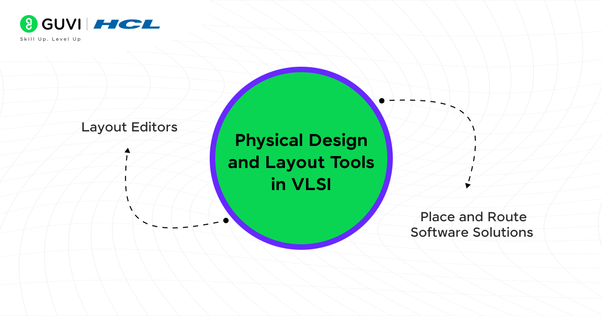
Layout refers to the geometrical representation of the chip, detailing the exact shapes, layers, and dimensions for transistors and interconnections.
It ensures manufacturability and compliance with design rules, making it a critical step before tape-out.
Physical implementation is a vital phase in your VLSI design experience. Abstract circuit descriptions evolve into manufacturable layouts during this stage.
Your success depends on selecting appropriate tools for placement, routing, and verification.
A) Place and Route Software Solutions
Place and Route (P&R) tools in VLSI design automate cell placement, interconnect routing, and optimization for power, performance, and area (PPA).

They ensure timing closure, manage congestion, and comply with design rules, enabling efficient layouts for advanced nodes. Let’s look at the top tools:
1. Synopsys IC Compiler II
Synopsys IC Compiler II is a premier physical design solution tailored for cutting-edge technology nodes, streamlining placement, routing, and optimization within a unified platform.
It ensures faster design convergence with enhanced quality of results (QoR) for high-speed and power-sensitive designs.
Key Features:
- Concurrent Clock and Data Optimization:
Simultaneously optimizes clock trees and data paths, reducing skew and enhancing timing performance. Ensures efficient clock distribution, even in complex designs.
- Machine Learning-Driven Placement Strategies:
Utilizes AI/ML algorithms to predict and refine placement decisions for better wirelength, congestion, and timing. Adapts to design-specific challenges, improving first-pass success rates.
- Advanced Integration for Smaller Nodes:
Supports advanced design rules and lithography requirements for 3nm and beyond, ensuring manufacturability.
Synopsys’ newer Fusion Compiler platform also integrates synthesis and place-and-route capabilities in an RTL-to-GDSII flow, making it increasingly important to understand alongside IC Compiler II.
2. Cadence Innovus
Cadence Innovus is a robust physical implementation tool designed to handle multi-million gate designs with precision.
Its emphasis on early optimization and scalability makes it a preferred choice for large-scale, power-efficient projects.
Key Features:
- Early Power Optimization:
Identifies and mitigates power inefficiencies during the early stages of physical implementation. Balances power and performance trade-offs to meet stringent low-power design requirements.
- Hierarchical Design Handling:
Efficiently manages large and complex SoCs by dividing them into hierarchical blocks for streamlined implementation. Ensures consistency and seamless integration between blocks.
- Support for Multi-Million Gate Designs:
Scales effortlessly for the largest and most intricate designs, maintaining high throughput and accuracy.
B) Layout Editors
Layout Editors and Verification Tools in VLSI design enable efficient creation and validation of IC layouts. These tools ensure design compliance with manufacturing rules and optimize layouts for performance.
Popular solutions like Cadence Virtuoso and LayoutEditor offer advanced editing, real-time design rule checking (DRC), and support for industry-standard file formats like GDSII, let’s look at them in detail:
1. Cadence Virtuoso Layout Suite
The Cadence Virtuoso Layout Suite is a premier tool for schematic-driven layout (SDL) design, catering to analog, digital, and mixed-signal circuits.
It accelerates design cycles by integrating layout creation, verification, and optimization on a unified platform.
Key Features:
- Real-Time Connectivity-Driven DRC:
Ensures designs adhere to foundry-specific rules while being created. Flags errors instantly during layout edits, preventing costly redesigns later in the flow.
- Advanced Automation Features:
Includes automated placement, routing, and floorplanning to streamline the creation of complex layouts. Features like module generators and parameterized cells (PCells) significantly reduce manual effort.
- Integrated Verification and Analysis:
Seamlessly connects with parasitic extraction tools and simulation environments for in-design analysis. Allows iterative optimization of performance metrics like timing, power, and area directly in the layout.
2. LayoutEditor
LayoutEditor is a versatile layout design tool known for its simplicity and adaptability across industries like MEMS, photonics, and IC design.
Its minimalistic interface coupled with robust functionality makes it a go-to choice for custom applications.
Key Features:
- Multi-Layer Editing Capabilities:
Supports editing across numerous layers simultaneously, which is vital for multilayer designs in advanced technologies. Offers layer-specific visibility and attributes to simplify complex layout views.
- GDSII Support:
Fully supports the GDSII format, the de facto standard for layout data exchange. Provides easy import/export options for smooth collaboration with other design tools.
- Customization and Extensibility:
Includes support for scripting in Python and other languages, allowing designers to create custom workflows.
Enables extensions and plug-ins for task-specific enhancements like batch processing and advanced rule checks.
4. Verification and Testing Tools
The physical design finalization leads to detailed verification that ensures your chip meets all specifications.
Your verification toolkit must address everything in three areas: functional correctness, timing constraints, and power requirements.
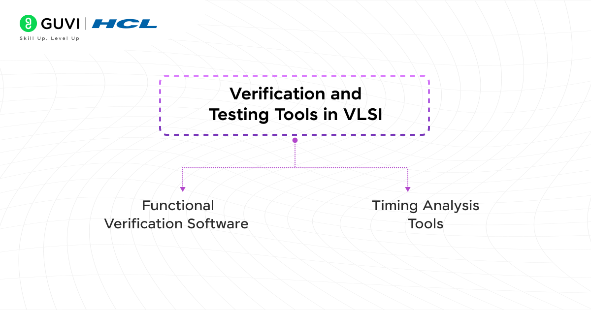
A) Functional Verification Software
Functional verification tools ensure that the design behaves as expected under all possible scenarios. This involves extensive simulation and debugging to identify errors in the logic or control flows.
Two leading tools in this category are VCS by Synopsys and Cadence Functional Verification Suite.
1. VCS by Synopsys
VCS (Verification Compiler Simulator) by Synopsys is a high-performance simulation tool designed to handle the complexities of modern chip designs.
It supports multiple languages, including SystemVerilog, and offers integrated debugging capabilities.
Key Features:
- Native Multicore Processor Support:
Leverages Fine-Grained Parallelism technology, enabling faster simulation times by distributing tasks across multiple CPU cores.
- Comprehensive SystemVerilog Support:
Provides extensive support for advanced verification methodologies, enhancing test coverage and efficiency.
- Verdi Debug System Integration:
Seamlessly integrates with the Verdi debug system, allowing engineers to visualize, trace, and debug simulation results efficiently.
2. Cadence Functional Verification Suite
This suite offers a robust environment for systematic and comprehensive functional verification. It simplifies the verification process by adhering to industry-standard methodologies like UVM.
Key Features:
- UVM Framework:
Supports the Universal Verification Methodology, a modular and reusable approach to functional verification, ensuring consistency across projects.
- Systematic Test Case Development:
Enables the creation of structured test cases that target specific functionalities, reducing the likelihood of missed bugs.
- Performance Optimization:
Incorporates advanced algorithms to optimize verification speed, ensuring faster design cycles.\
3. Siemens Questa
Questa provides simulation and verification capabilities for HDL-based digital designs.
In 2026, Siemens is also expanding AI-assisted verification through its Questa One and agentic AI initiatives.
B) Timing Analysis Tools
Timing verification ensures that signals propagate correctly within the specified timing constraints.
Static Timing Analysis (STA) tools analyze these constraints without requiring extensive simulations. Leading tools include Cadence Tempus and Synopsys PrimeTime.
1. Cadence Tempus
Cadence Tempus is a scalable STA tool designed for large-scale designs. It helps achieve timing closure efficiently by providing hierarchical abstraction and advanced timing analysis capabilities.
Key Features:
- Production-Proven Capacity:
Handles designs with over 1 billion instances, making it suitable for large and complex VLSI systems.
- SmartScope Technology:
Offers hierarchical abstraction, simplifying timing closure by focusing on critical timing paths while abstracting less critical areas.
- Aging-Aware STA:
Incorporates aging effects for applications in automotive and aerospace, ensuring long-term reliability.
2. Synopsys PrimeTime
Synopsys PrimeTime is a widely used STA tool that provides accurate timing analysis and signoff. Its advanced features go beyond basic timing checks.
Key Features:
- HSPICE-Accurate Signoff Analysis:
Ensures highly precise timing validation, critical for designs with stringent timing margins.
- Multi-Scenario Analysis:
Evaluates the design under multiple operational scenarios to ensure robustness across varying conditions.
- Advanced On-Chip Variation Support:
Models manufacturing variations to improve the accuracy of timing predictions.
These tools work together to enhance your verification process. To cite an instance, functional verification identifies logical errors, timing analysis confirms performance requirements, and power analysis tools optimize energy consumption.
This integrated approach helps deliver reliable, high-performance chips that meet specifications.
Top VLSI Design Tools Comparison in 2026
If you want a quick overview of which tool is used for what, this table provides the answer:
| VLSI Design Tool | Vendor | Main Use | Best Suited For |
| Virtuoso | Cadence | Custom IC design & layout | Analog/Mixed-Signal |
| Spectre | Cadence | Circuit simulation | Analog VLSI |
| Genus | Cadence | RTL synthesis | Digital VLSI |
| Innovus | Cadence | Physical implementation | Physical Design |
| Tempus | Cadence | Static timing analysis | STA/Sign-off |
| Xcelium | Cadence | Digital simulation | Verification |
| Cerebrus | Cadence | AI-driven optimization | Advanced Design |
| Design Compiler NXT | Synopsys | RTL synthesis | Digital VLSI |
| Fusion Compiler | Synopsys | RTL-to-GDSII implementation | Physical Design |
| IC Compiler II | Synopsys | Physical implementation | Backend VLSI |
| VCS | Synopsys | Simulation | Verification |
| PrimeTime | Synopsys | Static timing analysis | Timing Sign-off |
| DSO.ai | Synopsys | AI-driven optimization | Design Exploration |
| Questa | Siemens EDA | Simulation & verification | Verification |
| Calibre | Siemens EDA | DRC/LVS & physical verification | Sign-off |
| Aprisa | Siemens EDA | Digital implementation | Physical Design |
| Tessent | Siemens EDA | Design-for-test | DFT |
| OpenROAD | Open Source | RTL-to-GDS implementation | Learning/Research |
Best VLSI Design Tools in India in 2026
India’s semiconductor ecosystem is creating greater demand for chip-design skills, making industry-standard EDA tools increasingly relevant for students, researchers, and aspiring VLSI engineers.
The Government of India’s Chips to Startup (C2S) Programme provides participating academic and R&D institutions with centralized access to EDA tools from vendors including Synopsys, Cadence, Siemens, Ansys, Keysight, Silvaco, and others.
The C2S portal’s 2026 statistics also track usage of EDA tools from Synopsys, Cadence, Siemens, Keysight, Ansys, Cadre, Silvaco, Compcarta, and Renesas-Altium.
The ChipIN Centre at C-DAC Bangalore provides centralized EDA infrastructure for the semiconductor design community and supports access to tools for IC design workflows.
Which VLSI Design Tools Should Indian Students Learn?
The answer depends on your specialization.
| Career Goal | Tools/Skills to Prioritize |
| RTL Design | Verilog, SystemVerilog, simulation, synthesis |
| Verification | SystemVerilog, UVM, VCS/Questa/Xcelium |
| Physical Design | Innovus / IC Compiler II / Fusion Compiler |
| Analog VLSI | Virtuoso + Spectre |
| STA | PrimeTime / Tempus |
| DFT | Tessent and DFT fundamentals |
| Physical Verification | Calibre and DRC/LVS concepts |
| FPGA Design | Vivado and HDL fundamentals |
| Open-Source VLSI | OpenROAD |
The important point is that you do not need to learn every EDA tool to start a VLSI career.
Choose a specialization and become comfortable with the tools used in that workflow.
Concluding Thoughts…
Modern VLSI design just needs sophisticated tools that match chip development’s growing complexity. Leading companies like Synopsys, Cadence, and Siemens EDA provide powerful solutions at different design stages, as shown in this detailed guide.
Commercial EDA suites deliver strong capabilities. Open-source alternatives now offer viable options for specific design tasks. Major vendors’ cloud-based solutions have changed accessibility. You can scale resources based on project needs and reduce infrastructure costs.
Your VLSI design workflow gets better with specialized tools at each stage.
AI-powered VLSI design tools are the next frontier in VLSI design automation. Solutions like DSO.ai and Cerebrus show most important improvements in design optimization. They reduce cell areas and improve runtime performance. These advances hint at what a world of artificial intelligence handling complex aspects of chip design might look like.
FAQs
1. What are the essential software VLSI design tools in 2026?
The essential VLSI design tools depend on the design stage. Major tools include Synopsys Design Compiler NXT, Fusion Compiler, VCS and PrimeTime; Cadence Virtuoso, Genus, Innovus, Xcelium and Tempus; and Siemens EDA tools such as Questa, Calibre, Aprisa and Tessent. OpenROAD is also useful for open-source digital design and research.
2. How has artificial intelligence impacted VLSI design tools?
AI has significantly enhanced VLSI design tools, improving efficiency and optimization. AI-powered tools like Synopsys DSO.ai and Cadence Cerebrus offer faster runtimes, improved cell area reduction, and automated design space exploration. These tools use machine learning algorithms to enhance various design stages, from layout synthesis to verification.
3. What are the key components of a modern VLSI design workflow?
A modern VLSI design workflow typically includes RTL design and synthesis tools, physical design and layout software, and comprehensive verification and testing tools. This encompasses HDL simulation, logic synthesis, place and route solutions, DRC/LVS tools, functional verification software, timing analysis tools, and power analysis and optimization solutions.
4. How do cloud-based EDA solutions benefit chip designers?
Cloud-based EDA solutions offer several advantages to chip designers, including faster time to results, pay-per-use pricing models, and the ability to scale computing resources on demand. They enable seamless collaboration across teams and provide access to massive computing capacity without the need for extensive on-premises infrastructure.
5. What are the differences between commercial and open-source EDA tools for VLSI design?
Commercial EDA tools from vendors like Synopsys and Cadence offer comprehensive, integrated solutions with extensive support and regular updates. They are typically more robust and feature-rich but come with high licensing costs. Open-source alternatives, while cost-effective and flexible, may lack some advanced features and industry-standard support. However, they are continually improving and can be suitable for specific design tasks or academic purposes.
6. Which VLSI design tools is best for beginners?
There is no single best VLSI tool for every beginner. For digital VLSI, start with Verilog/SystemVerilog and simulation before moving into synthesis and physical design. For analog VLSI, Cadence Virtuoso is an important tool to learn. OpenROAD can also provide an accessible option for learning digital implementation concepts.
7. Which software is used for VLSI physical design?
Popular VLSI physical-design tools include Cadence Innovus, Synopsys IC Compiler II, Synopsys Fusion Compiler, and Siemens Aprisa. They support activities such as floorplanning, placement, clock-tree synthesis, routing, and optimization.
8. Which tools are used for VLSI verification?
Common VLSI verification tools include Synopsys VCS, Cadence Xcelium, and Siemens Questa. Engineers also use SystemVerilog, UVM, assertions, functional coverage, debugging, and formal verification methodologies.
9. Which software is used for VLSI layout design?
Cadence Virtuoso is one of the most important tools for analog and custom IC layout. Physical-verification tools such as Siemens Calibre and Cadence solutions are then used for checks such as DRC and LVS.
10. Is Cadence or Synopsys better for VLSI?
Neither is universally better. Both provide extensive EDA ecosystems. The better option depends on your role and the design flow used by the organization. Cadence has strong offerings across custom IC design and digital implementation, while Synopsys provides major solutions across synthesis, simulation, physical implementation, timing, verification, and AI-driven optimization.
11. Which VLSI design tools should I learn for a job in India?
Choose VLSI design tools based on your specialization:
RTL Design: Verilog, SystemVerilog, synthesis tools
Verification: SystemVerilog, UVM, VCS/Questa/Xcelium
Physical Design: Innovus, IC Compiler II, or Fusion Compiler
Analog Design: Virtuoso and Spectre
STA: PrimeTime or Tempus
DFT: Tessent and DFT fundamentals
Physical Verification: Calibre and DRC/LVS concepts
Most importantly, combine tool knowledge with strong VLSI fundamentals and hands-on projects.
Success Stories

About the Author
Jaishree Tomar
A recent CS Graduate with a quirk for writing and coding, a Data Science and Machine Learning enthusiast trying to pave my own way with tech. I have worked as a freelancer with a UK-based Digital Marketing firm writing various tech blogs, articles, and code snippets. Now, working as a Technical Writer at GUVI writing to my heart’s content!
View all posts by Jaishree Tomar
Connect with me @













Did you enjoy this article?