


VLSI Design Articles
Why Chips Fail: A Basic Guide to Chip Defects and IC Failure Analysis
Fun Facts About the Semiconductor Industry
Why Are Semiconductor Chips Expensive? Manufacturing Cost Explained
Instruction Set Architecture: How ISA Shapes Modern Chip Design


Get In Touch For Details! Request More Information
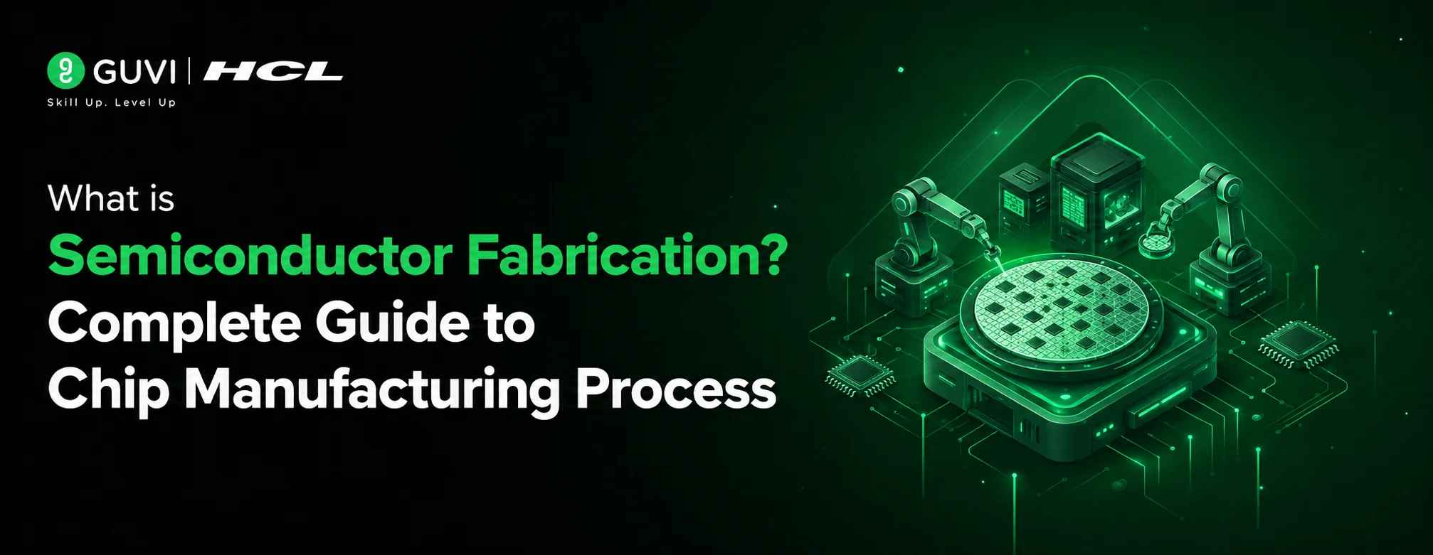
What is Semiconductor Fabrication? Complete Guide to Chip Manufacturing Process
Aug 03, 2026 8 Min Read 377 Views
(Last Updated)
Table of contents
- TL;DR Summary
- What is Semiconductor Fabrication?
- Definition in Simple Terms
- The Scale of Modern Fabrication
- Why is Semiconductor Fabrication Important?
- Powering Every Industry
- Economic Impact
- Did You Know?
- The Semiconductor Manufacturing Process Step-by-Step
- Stage 1: Wafer Preparation
- Stage 2: Photolithography
- Stage 3: Etching
- Stage 4: Doping and Ion Implantation
- Stage 5: Thin Film Deposition
- Stage 6: Chemical Mechanical Planarization (CMP)
- Stage 7: Metallization
- Stage 8: Wafer Testing
- Stage 9: Packaging and Assembly
- Stage 10: Final Testing
- Key Components in the Fabrication Process
- Cleanroom Environment
- Specialized Equipment
- Process Chemicals
- Semiconductor Foundry: Where Chips Are Born
- Pure-Play Foundries
- Integrated Device Manufacturers (IDMs)
- Fabless Companies
- Foundry Economics
- Challenges in Chip Fabrication
- Miniaturization Limits
- Yield Management
- Cost Escalation
- Supply Chain Complexity
- Environmental Concerns
- Real-World Examples of Semiconductor Fabrication
- TSMC: The Foundry Leader
- Intel: IDM Transformation
- Samsung: Memory and Foundry
- India's Semiconductor Ambitions
- Common Mistakes to Avoid When Learning Semiconductor Fabrication
- Underestimating the Complexity
- Ignoring the Cleanroom Importance
- Confusing Process Nodes with Physical Dimensions
- Neglecting Packaging and Testing
- Overlooking Industry Trends
- Career Opportunities in Semiconductor Manufacturing
- Growing Demand
- Key Job Roles
- Salary Prospects
- How to Get Started as a VLSI Engineer?
- Ready to launch your career in semiconductor design?
- Conclusion
- Frequently Asked Questions
- What is semiconductor fabrication?
- How long does the semiconductor fabrication process take?
- What is the difference between wafer fabrication and chip fabrication?
- Why are cleanrooms necessary for semiconductor manufacturing?
- What is a semiconductor foundry?
- How much does a semiconductor fabrication plant cost?
- What career opportunities exist in semiconductor manufacturing?
- What is the role of photolithography in semiconductor fabrication?
- What are the main challenges in semiconductor manufacturing?
- How is India positioning itself in semiconductor manufacturing?
TL;DR Summary
- Semiconductor fabrication is the intricate process of manufacturing integrated circuits (ICs) on silicon wafers.
- It involves transforming raw silicon into functional chips through multiple precise steps, including wafer preparation, photolithography, etching, doping, and packaging.
- This process takes place in highly controlled cleanroom environments where a single dust particle can ruin an entire batch.
- Understanding this process is essential for anyone pursuing a career in VLSI design or semiconductor manufacturing.
Every electronic device you use today- your smartphone, laptop, car, and even your washing machine contains semiconductor chips. These tiny silicon marvels power our digital world. But have you ever wondered how these chips are actually made?
The process of creating these chips is called semiconductor fabrication. It’s one of the most sophisticated manufacturing processes humans have ever developed. A single modern processor contains billions of transistors, each smaller than a virus, all precisely arranged on a piece of silicon no larger than your fingernail.
This guide will walk you through everything you need to know about semiconductor fabrication and give you a solid foundation.
What is Semiconductor Fabrication?
Semiconductor fabrication is the manufacturing process of creating integrated circuits on semiconductor wafers. The process transforms raw silicon into functional electronic chips that power everything from simple calculators to complex artificial intelligence systems.
The fabrication process takes place in specialized facilities called fabrication plants or “fabs.” These fabs maintain ultra-clean environments where temperature, humidity, and particle contamination are strictly controlled.
Definition in Simple Terms
Think of semiconductor fabrication like printing a newspaper, but at a microscopic scale. Instead of ink on paper, you’re using light, chemicals, and conductive materials to print electronic circuits on silicon wafers.
The process involves layering different materials on a silicon wafer and then etching patterns to create transistors, resistors, capacitors, and their interconnections. Each layer adds specific functionality to the final chip.
The Scale of Modern Fabrication
Modern chip fabrication operates at an incredible scale. Today’s most advanced chips use process nodes like 3nm or 5nm, meaning the smallest features on the chip are just 3 to 5 nanometers wide.
For perspective, a human hair is about 80,000 nanometers thick. A red blood cell is approximately 7,000 nanometers. This extreme miniaturization is what makes semiconductor fabrication so challenging and fascinating.
If you’re new to semiconductors, start by understanding how semiconductor technology evolved from silicon to modern AI processors before exploring the manufacturing process.
Why is Semiconductor Fabrication Important?
Semiconductor fabrication forms the backbone of modern technology. Without it, we wouldn’t have smartphones, computers, medical devices, or even modern automobiles.
Powering Every Industry
The chips produced through wafer fabrication are essential across every sector:
- Consumer Electronics: Smartphones, laptops, tablets, smartwatches
- Automotive: Engine control units, infotainment systems, autonomous driving
- Healthcare: Medical imaging devices, pacemakers, diagnostic equipment
- Telecommunications: 5G infrastructure, routers, satellites
- Aerospace: Navigation systems, flight controls, satellite communications
Economic Impact
The semiconductor industry is massive. According to Market Us, the global semiconductor market size was valued at USD 840.60 billion in 2024 and is predicted to reach approximately USD 2,010.6 billion by 2034. This growth is driven by increasing demand for AI chips, IoT devices, and electric vehicles.
Countries around the world are investing heavily in domestic semiconductor manufacturing capabilities. The United States, China, Taiwan, South Korea, and Japan are leading the global race for chip production supremacy.
Did You Know?
The entire semiconductor fabrication process for one chip can involve over 1,000 individual steps and take more than three months to complete.
Fabrication is one stage of the overall semiconductor value chain. Before manufacturing begins, chips go through design, verification, and physical implementation. To know that in detail, read our blog on “Semiconductor Value Chain Explained: From Design to Delivery”.
The Semiconductor Manufacturing Process Step-by-Step
The fabrication process involves hundreds of individual steps and can take more than three months from start to finish. Let’s break down the major stages.
Stage 1: Wafer Preparation
The process begins with creating silicon wafers, the foundation for all semiconductor chips.
Raw Material Processing
Silicon is extracted from sand and purified to extremely high levels with 99.9999999% purity. This ultra-pure silicon is then melted and formed into large cylindrical ingots through a process called the Czochralski method.
These silicon ingots are then sliced into thin wafers using diamond-tipped saws. A typical wafer is about 0.7mm thick and can be 200mm or 300mm in diameter.
Wafer Polishing
The sliced wafers undergo extensive polishing to create a mirror-smooth surface. Any imperfection at this stage could cause defects in the final chips, so this step is critical.
Stage 2: Photolithography
Photolithography is the cornerstone of the chip fabrication process. It’s similar to photography but at a microscopic scale.
Photoresist Application
A light-sensitive material called photoresist is applied to the wafer surface. This material changes its chemical properties when exposed to light.
Mask Alignment and Exposure
A photomask, a glass plate with the circuit pattern is aligned over the wafer. Ultraviolet light is then shone through the mask, transferring the pattern onto the photoresist.
Development
The exposed photoresist is developed, washing away either the exposed or unexposed areas depending on whether a positive or negative resist was used. This creates the pattern that will be etched into the silicon.
Stage 3: Etching
Etching removes material from the wafer to create the circuit patterns defined during photolithography.
Wet Etching
This method uses liquid chemicals to dissolve unwanted material. It’s relatively simple but can undercut the photoresist mask.
Dry Etching
Dry etching uses plasma or gas-phase chemicals. It provides better control and is used for creating finer features in modern chips.
Stage 4: Doping and Ion Implantation
Doping introduces impurities into specific regions of the silicon to modify its electrical properties.
Purpose of Doping
Pure silicon is a semiconductor, meaning its conductivity can be controlled. Adding specific impurities creates regions that conduct electricity differently, essential for building transistors.
Ion Implantation
This technique accelerates dopant ions and shoots them into the silicon wafer. The ions penetrate the surface to a controlled depth, creating precisely doped regions.
Stage 5: Thin Film Deposition
Multiple layers of different materials are deposited on the wafer to create insulation, conductive pathways, and other structures.
Chemical Vapor Deposition (CVD)
Gases react on the wafer surface to deposit thin films of materials like silicon dioxide, silicon nitride, or metal.
Physical Vapor Deposition (PVD)
Material is physically ejected from a target and deposited onto the wafer. This is commonly used for metal layers like aluminum or copper.
Stage 6: Chemical Mechanical Planarization (CMP)
Each layer must be perfectly flat before the next layer can be added. CMP polishes the wafer surface using a combination of chemical reactions and mechanical abrasion.
Stage 7: Metallization
Metal layers are added to connect different components of the circuit.
Interconnect Formation
Copper or aluminum is deposited and patterned to create the wiring that connects transistors and other components. Modern chips can have 10-15 metal layers stacked on top of each other.
Stage 8: Wafer Testing
Before further processing, each chip on the wafer is tested for functionality.
Electrical Testing
Specialized probe stations contact the bonding pads on each chip and run electrical tests. Defective chips are marked and will not be packaged.
Stage 9: Packaging and Assembly
The tested wafers are then prepared for final use.
Die Separation
The wafer is cut into individual chips (dies) using a diamond saw or laser.
Packaging
Each die is mounted in a protective package that provides electrical connections and thermal management. Common package types include:
- BGA (Ball Grid Array)
- QFN (Quad Flat No-leads)
- Flip-chip packages
Stage 10: Final Testing
The packaged chips undergo final testing to ensure they meet specifications for performance, power consumption, and reliability.
Key Components in the Fabrication Process
Several critical elements make semiconductor manufacturing possible.
Cleanroom Environment
Semiconductor fabs operate in ISO Class 4-6 cleanrooms. These environments maintain particle levels between 352 and 35,200 particles per cubic meter at 0.5 μm, compared to millions of particles in normal air.
A single dust particle can short-circuit a chip. That’s why fab workers wear full-body “bunny suits,” and the air is constantly filtered and recirculated.
The cleanroom air in a semiconductor fab is 1,000 to 10,000 times cleaner than a hospital operating room.
Specialized Equipment
The semiconductor manufacturing equipment market is substantial. Semiconductor manufacturing was valued at USD 118.88 billion in 2025 and is projected to reach USD 224.93 billion by 2033.
Key equipment includes:
- Steppers and Scanners: For photolithography
- Etching Systems: For removing material
- Deposition Systems: For adding thin films
- Inspection Tools: For defect detection
- Metrology Equipment: For measuring dimensions
Process Chemicals
The fabrication process uses hundreds of different chemicals, including:
- Ultra-pure water
- Specialty gases (argon, nitrogen, oxygen)
- Photoresist chemicals
- Etching solutions
- Cleaning solvents
A modern semiconductor fab uses more ultra-pure water in a day than a small city consumes. The water must be purified to a resistivity of 18.2 MΩ·cm, purer than distilled water.
Semiconductor Foundry: Where Chips Are Born
A semiconductor foundry is a specialized facility that manufactures chips designed by other companies. This business model separates chip design from manufacturing.
Pure-Play Foundries
Companies like TSMC (Taiwan Semiconductor Manufacturing Company) operate as pure-play foundries. They don’t design chips, they only manufacture them for clients.
TSMC dominates the foundry market with approximately 73% market share in Q1 2026. Samsung Foundry holds about 7%, while other players like SMIC and UMC make up the remainder.
Integrated Device Manufacturers (IDMs)
Companies like Intel and Samsung design and manufacture their own chips. They have their own fabs but may also use foundries for additional capacity.
Fabless Companies
Companies like NVIDIA, AMD, and Apple design chips but don’t own manufacturing facilities. They rely entirely on foundries like TSMC for production.
Foundry Economics
Building a modern semiconductor fab is expensive. A state-of-the-art facility can cost $10-20 billion or more. This high barrier to entry is why many companies choose the fabless model.
Challenges in Chip Fabrication
Semiconductor fabrication faces numerous technical and economic challenges.

Miniaturization Limits
As transistors shrink to atomic scales, physical limitations emerge. Quantum effects, electron tunneling, and heat dissipation become major concerns.
Yield Management
Not all chips on a wafer work correctly. The yield, the percentage of functional chips, directly impacts profitability. Advanced process nodes often have initial yields below 50%, gradually improving as the process matures.
Cost Escalation
The cost of developing new process nodes increases dramatically. TSMC’s 3nm wafers cost approximately $ 19,500 each, compared to $ 3,000 for mature 28nm wafers.
Supply Chain Complexity
The semiconductor supply chain spans the globe. Raw materials come from one country, equipment from another, manufacturing in a third, and assembly elsewhere. This creates vulnerabilities to geopolitical disruptions.
Environmental Concerns
Semiconductor manufacturing consumes significant energy and water. A modern fab can use 2-4 million gallons of ultra-pure water daily. The industry is working to reduce its environmental footprint.
Real-World Examples of Semiconductor Fabrication
Let’s look at how major companies approach semiconductor manufacturing.
TSMC: The Foundry Leader
TSMC operates multiple fabs across Taiwan and is expanding globally. Their 3nm process is the most advanced in mass production, used for chips in iPhones, Macs, and data center processors.
TSMC’s success comes from continuous innovation and close collaboration with customers. They invest billions annually in R&D and new fab construction.
Intel: IDM Transformation
Intel is transitioning from pure IDM to offering foundry services. Their Intel Foundry Services division aims to compete with TSMC by manufacturing chips for external customers.
This strategic shift addresses two needs: utilizing their fab capacity more efficiently and participating in the growing foundry market.
Samsung: Memory and Foundry
Samsung operates as both an IDM and foundry. They’re the world’s largest memory chip manufacturer and a significant player in logic foundry services.
Samsung’s advanced nodes compete directly with TSMC, offering alternatives for companies seeking supply chain diversification.
India’s Semiconductor Ambitions
India is investing heavily in developing domestic semiconductor manufacturing. The government’s Semiconductor Mission aims to establish fabrication facilities and create a complete ecosystem.
Several projects are underway, including facilities by Tata Group and international partnerships. India aims to become a major player in global semiconductor manufacturing by 2030.
Learn how India’s Semiconductor Mission is building fabs, attracting global investments, and creating thousands of VLSI jobs.
A single modern smartphone processor contains over 10 billion transistors. If you could lay these transistors side by side, they would stretch around the Earth’s equator multiple times.
Common Mistakes to Avoid When Learning Semiconductor Fabrication
Understanding semiconductor manufacturing can be challenging. Here are common mistakes learners make:
1. Underestimating the Complexity
Many beginners think chip fabrication is similar to printed circuit board (PCB) manufacturing. In reality, semiconductor fabrication operates at scales 1,000 times smaller and involves fundamentally different physics.
Avoid this by: Studying the physics behind each process step, not just the procedures.
2. Ignoring the Cleanroom Importance
Students often focus on the process steps while underestimating the cleanroom environment’s role. Without proper contamination control, even perfect process execution fails.
Avoid this by understanding cleanroom classifications and contamination sources before diving into process details.
3. Confusing Process Nodes with Physical Dimensions
A “5nm process node” doesn’t mean features are 5nm in size. Node names have become marketing terms rather than precise measurements.
Avoid this by: Learning actual dimensions of transistors, metal pitch, and other relevant metrics.
4. Neglecting Packaging and Testing
Many learners focus entirely on wafer fabrication while ignoring packaging and testing. These steps significantly impact final chip performance and reliability.
Avoid this by: Studying the complete manufacturing flow from silicon to finished product.
5. Overlooking Industry Trends
Semiconductor technology evolves rapidly. Learning from outdated materials can lead to misconceptions about current capabilities.
Avoid this by: Following industry news, reading recent technical papers, and staying updated on process technology advancements.
Career Opportunities in Semiconductor Manufacturing
The semiconductor industry offers excellent career prospects for engineers.
Growing Demand
India is expected to need approximately 10 lakh (1 million) VLSI engineers by 2027. This demand spans design, verification, testing, and manufacturing roles.
Key Job Roles
- VLSI Design Engineer: Designs digital and analog circuits
- Process Engineer: Develops and optimizes fabrication processes
- Yield Engineer: Improves manufacturing yield and quality
- Test Engineer: Develops testing methodologies and equipment
- Packaging Engineer: Designs chip packages and assembly processes
- Equipment Engineer: Maintains and improves fab equipment
If you’re wondering which semiconductor specialization suits your interests, explore the major VLSI domains before choosing a career path.
Salary Prospects
VLSI engineers in India can expect starting salaries of ₹6-12 lakhs per annum for freshers, with experienced professionals earning ₹25-50 lakhs or more annually.
How to Get Started as a VLSI Engineer?
A strong foundation in electronics, solid-state physics, and semiconductor devices is essential. Specialized training through courses like a VLSI Design Course can provide the practical skills needed to enter this field.
Ready to launch your career in semiconductor design?
HCL GUVI’s VLSI Design Course provides comprehensive training in semiconductor fundamentals, Verilog HDL, digital design, and industry-standard tools. With hands-on projects and expert mentorship, you’ll gain the practical skills that semiconductor companies actively seek.
Whether you’re a recent graduate or a working professional looking to specialize, this course will prepare you for roles in chip design, verification, and physical design. Join thousands of learners who’ve successfully transitioned into the semiconductor industry.
Explore the VLSI Design Course Today →
Conclusion
Semiconductor fabrication is the foundation of modern electronics. This complex process transforms raw silicon into the powerful chips that run our digital world. From wafer preparation through photolithography, etching, doping, and packaging, each step requires incredible precision and control.
Understanding semiconductor manufacturing opens doors to exciting career opportunities. As the demand for more powerful, efficient chips grows, so does the need for skilled professionals in this field.
Learning about semiconductor fabrication is the first step toward participating in one of humanity’s most impressive manufacturing achievements. Consider building your expertise through structured learning like a VLSI Design Course to turn this knowledge into a rewarding career.
Frequently Asked Questions
1. What is semiconductor fabrication?
Semiconductor fabrication is the manufacturing process of creating integrated circuits on silicon wafers. It involves multiple steps including wafer preparation, photolithography, etching, doping, and packaging to transform raw silicon into functional electronic chips.
2. How long does the semiconductor fabrication process take?
The complete semiconductor fabrication process can take more than three months from start to finish. This includes over 1,000 individual steps across wafer manufacturing, chip fabrication, testing, and packaging stages.
3. What is the difference between wafer fabrication and chip fabrication?
Wafer fabrication refers specifically to creating the silicon wafer itself from raw silicon. Chip fabrication is the broader process of creating integrated circuits on those wafers. Often, these terms are used interchangeably to describe the complete manufacturing process.
4. Why are cleanrooms necessary for semiconductor manufacturing?
Cleanrooms are essential because even microscopic dust particles can destroy a chip. Semiconductor features are measured in nanometers, and a single particle can short-circuit connections. Cleanrooms maintain particle levels up to 10,000 times cleaner than hospital operating rooms.
5. What is a semiconductor foundry?
A semiconductor foundry is a specialized facility that manufactures chips designed by other companies. Pure-play foundries like TSMC only manufacture chips; they don’t design them. This allows fabless companies like Apple and NVIDIA to focus on design while foundries handle production.
6. How much does a semiconductor fabrication plant cost?
A modern semiconductor fabrication plant costs between $10-20 billion or more. The expense comes from advanced equipment, cleanroom facilities, and sophisticated infrastructure. This high cost is why many use foundries rather than building their own fabs.
7. What career opportunities exist in semiconductor manufacturing?
Career opportunities include VLSI design engineer, process engineer, yield engineer, test engineer, packaging engineer, and equipment engineer roles. India alone needs approximately 1 million VLSI engineers by 2027, offering excellent salary prospects and growth potential.
8. What is the role of photolithography in semiconductor fabrication?
Photolithography transfers circuit patterns onto silicon wafers using light-sensitive materials and photomasks. It’s the fundamental process that defines where transistors and interconnections are created. Modern photolithography uses extreme ultraviolet (EUV) light to create features smaller than 10 nanometers.
9. What are the main challenges in semiconductor manufacturing?
Key challenges include miniaturization limits at atomic scales, maintaining high yield rates, escalating costs of advanced process nodes, complex global supply chains, and environmental concerns including high energy and water consumption.
10. How is India positioning itself in semiconductor manufacturing?
India is investing heavily in domestic semiconductor manufacturing through the Semiconductor Mission. Projects by the Tata Group and international partnerships aim to establish fabrication facilities. India targets becoming a significant global semiconductor manufacturing hub by 2030.
Success Stories

About the Author
Hashmithaa
Hi, I’m Hashmithaa — a content writer with a love for words. Writing isn’t just what I do; it’s how I connect, communicate, and create meaning in a noisy digital world. And if my words help someone make a better decision, learn something new, or feel more confident, then I’ve done my job well.
View all posts by Hashmithaa
Connect with me @










Did you enjoy this article?