


VLSI Design Articles
Why Chips Fail: A Basic Guide to Chip Defects and IC Failure Analysis
Fun Facts About the Semiconductor Industry
Why Are Semiconductor Chips Expensive? Manufacturing Cost Explained
Instruction Set Architecture: How ISA Shapes Modern Chip Design

Get In Touch For Details! Request More Information
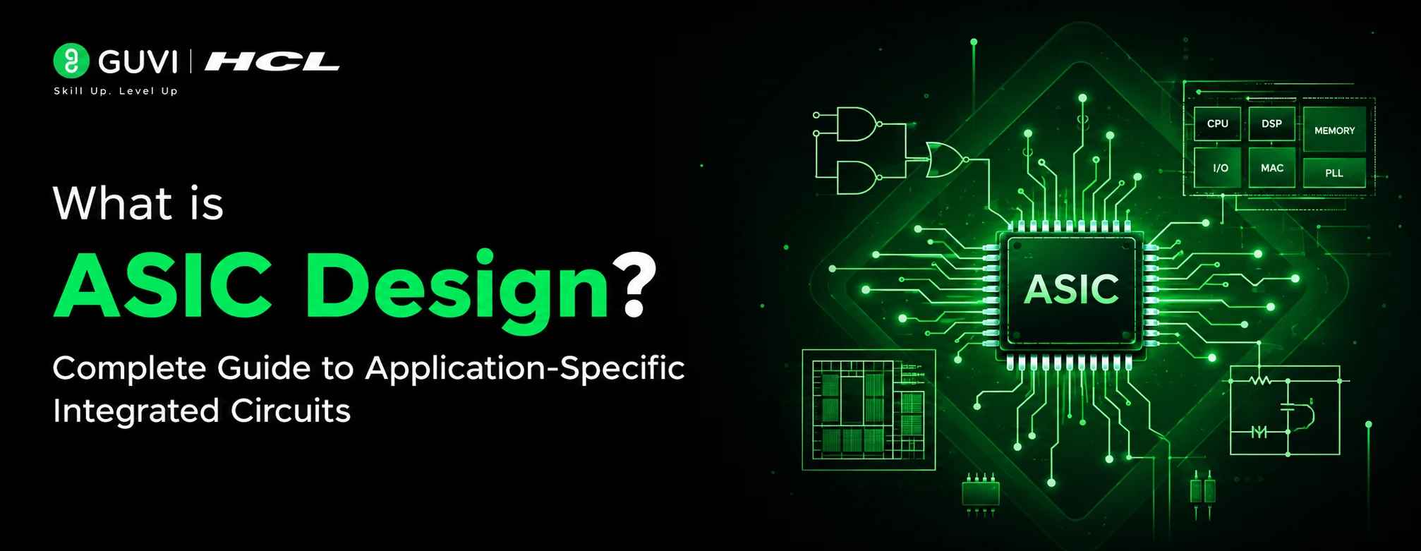
What is ASIC Design? Complete Guide to Application-Specific Integrated Circuits
Aug 03, 2026 6 Min Read 260 Views
(Last Updated)
Table of contents
- TL;DR Summary
- Introduction
- What is an Application-Specific Integrated Circuit?
- Key Characteristics of ASICs
- How ASICs Differ from General-Purpose Chips?
- Why ASIC Design Matters in Modern Electronics?
- Performance Optimization
- Power Efficiency
- Cost Reduction at Scale
- Competitive Advantage
- The Complete ASIC Design Flow
- Stage 1: Specification and Requirements
- Stage 2: Architecture Design
- Stage 3: RTL Design (Register Transfer Level)
- Stage 4: Functional Verification
- Stage 5: Synthesis
- Stage 6: Physical Design
- Stage 7: Tapeout and Fabrication
- Stage 8: Testing and Packaging
- Types of ASICs
- Full Custom ASIC
- Semi-Custom ASIC
- Platform-Based ASIC
- ASIC vs FPGA: Key Differences
- What is an FPGA?
- Comparison Table: ASIC vs FPGA
- When to Choose ASIC
- When to Choose FPGA?
- ASIC Design Lifecycle
- Popular ASIC Design Tools
- Real-World Applications of ASICs
- Smartphones
- Data Centers
- Cryptocurrency Mining
- Automotive
- Medical Devices
- Skills Required for ASIC Engineers
- Advantages and Disadvantages of ASIC Design
- Advantages of ASIC Design
- Disadvantages of ASIC Design
- Common Mistakes in ASIC Design
- Incomplete Specification
- Underestimating Verification Effort
- Ignoring Power Analysis Until Late
- Poor Clock Domain Crossing Handling
- Over-Optimizing for One Metric
- Career Opportunities in Custom IC Design
- Key Roles in ASIC Design
- Salary Expectations
- How to Start Your Career in Semiconductor Design?
- Ready to launch your career in semiconductor design?
- Conclusion
- Frequently Asked Questions
- What is ASIC design in simple terms?
- How long does ASIC design take?
- What is the difference between ASIC and FPGA?
- What skills are needed for ASIC design?
- How much does ASIC design cost?
- Why do companies use ASICs instead of general-purpose chips?
- What industries use ASICs most?
- Can ASIC design be learned online?
- What is the ASIC design flow?
- Is ASIC design a good career?
TL;DR Summary
- ASIC design refers to the process of creating Application-Specific Integrated Circuits: custom chips engineered for a single, dedicated purpose.
- Unlike general-purpose processors, ASICs deliver superior performance, lower power consumption, and optimized functionality for specific tasks.
- The ASIC design flow involves specification, architecture, logic design, verification, physical design, and fabrication.
- ASICs power everything from smartphones to AI accelerators, making ASIC design skills highly valuable in today’s semiconductor industry.
Introduction
Every electronic device you use today, from your smartphone to your car’s navigation system, relies on integrated circuits. But not all chips are created equal.
Some chips are designed to handle multiple tasks. Others are built for one specific purpose. That’s where ASIC design comes into the picture.
ASIC stands for Application-Specific Integrated Circuit. It’s a custom-designed chip created to perform a particular function with maximum efficiency.
Think of it like a specialized tool versus a Swiss Army knife. A Swiss Army knife does many things adequately. A specialized tool does one thing exceptionally well.
The global ASIC market was valued at USD 24.21 billion in 2026 and is projected to reach USD 41.68 billion by 2034, growing at a CAGR of 7%. This growth reflects the increasing demand for customized, high-performance chips across industries.
If you’re exploring a career in semiconductor design, understanding ASIC design is fundamental. This guide will walk you through everything you need to know from basic concepts to the complete design flow.
What is an Application-Specific Integrated Circuit?
An Application-Specific Integrated Circuit is a chip designed for a single, dedicated application rather than general-purpose use.
Unlike microprocessors or microcontrollers that can run various programs, an ASIC has its functionality hardwired into its physical structure.
Key Characteristics of ASICs
- Single-purpose design: Built to execute one specific task or set of tasks
- Custom architecture: The internal structure is optimized for the target application
- Non-programmable: Functionality cannot be changed after manufacturing
- High efficiency: Delivers superior performance per watt for the intended application
How ASICs Differ from General-Purpose Chips?
| Feature | General-Purpose IC | ASIC |
| Flexibility | High (programmable) | Low (fixed function) |
| Performance | Moderate | Optimized for specific task |
| Power Efficiency | Moderate | High for target application |
| Development Cost | Low | High (custom design) |
| Unit Cost | Moderate | Low (at high volumes) |
| Time to Market | Fast | Slow (months to years) |
The trade-off is clear: ASICs require significant upfront investment but deliver unmatched efficiency for high-volume applications.
Why ASIC Design Matters in Modern Electronics?
ASIC design has become the backbone of modern technology. Here’s why it matters:
1. Performance Optimization
When you design a chip for a specific purpose, every transistor serves that purpose.
General-purpose processors waste resources on flexibility they don’t need. ASICs eliminate this overhead.
For example, Bitcoin mining ASICs perform hashing operations 100,000 times faster than general-purpose CPUs while consuming a fraction of the power.
2. Power Efficiency
Power consumption is critical for mobile devices, IoT sensors, and data centers.
ASICs minimize power waste by implementing only the necessary functionality. A well-designed ASIC can reduce power consumption by 50-90% compared to general-purpose alternatives doing the same task.
3. Cost Reduction at Scale
The math is simple: high fixed cost, low variable cost.
Designing an ASIC costs 5−50 million upfront, but manufacturing each chip costs only 5−50 million upfront, but manufacturing each chip costs only 1-10 million at high volumes.
Once production exceeds 150,000-200,000 units, ASICs become far cheaper than FPGAs, which cost $50-500 per unit.
4. Competitive Advantage
Companies that develop proprietary ASICs gain significant advantages.
Apple’s custom chips (A-series, M-series) differentiate their products from competitors using off-the-shelf components. Google’s Tensor Processing Units (TPUs) give their AI services a performance edge.
The Complete ASIC Design Flow
The ASIC design flow is a systematic process that transforms a concept into a manufactured chip. It typically takes 12-24 months for complex designs.
Let’s break down each stage:
Stage 1: Specification and Requirements
Everything starts with defining what the chip must do. Engineers work with stakeholders to capture:
- Functional requirements (what the chip does)
- Performance targets (speed, throughput)
- Power budget (maximum power consumption)
- Area constraints (physical size limits)
- Cost targets (manufacturing budget)
This phase typically takes 4-8 weeks for complex designs.
Stage 2: Architecture Design
Architects make high-level decisions about the chip’s structure. Key decisions include:
- Processing elements and their organization
- Memory hierarchy and bandwidth
- Interface protocols (PCIe, USB, DDR)
- Clocking strategy
- Power domains
Architecture decisions impact everything that follows. A poor architecture cannot be fixed later without massive rework.
Stage 3: RTL Design (Register Transfer Level)
Engineers write the chip’s functionality in hardware description languages (HDL) like Verilog or VHDL.
At this stage, the design is:
- Written in synthesizable code
- Functionally correct but not yet physical
- Simulated to verify behavior
RTL design is where the logical functionality is captured. A typical complex ASIC may contain 10-100 million lines of RTL code.
Stage 4: Functional Verification
Verification ensures the design matches the specification. This is often the longest phase, consuming 50-70% of the total design effort.
Verification techniques include:
- Simulation (running test cases)
- Formal verification (mathematical proofs)
- Emulation (hardware-accelerated testing)
- FPGA prototyping (early silicon validation)
Stage 5: Synthesis
Synthesis converts RTL code into a gate-level netlist.
The synthesis tool:
- Maps RTL constructs to standard cell libraries
- Optimizes for area, timing, and power
- Generates timing constraints
The output is a netlist describing the chip as interconnected logic gates.
Stage 6: Physical Design
Physical design transforms the logical netlist into a manufacturable layout.
Key steps include:
- Floorplanning: Placing major blocks
- Placement: Positioning individual cells
- Clock tree synthesis: Distributing clock signals
- Routing: Connecting all components
- Signoff: Verifying timing, power, and manufacturability
Physical design directly impacts chip performance, power, and area (PPA).
Stage 7: Tapeout and Fabrication
“Tapeout” is the process of sending the final design data to the foundry for manufacturing.
The fabrication process:
- Creates photomasks (optical templates)
- Etches patterns onto silicon wafers
- Builds multiple layers of transistors and wiring
- Takes 8-16 weeks for advanced nodes
Modern chips use process nodes as small as 3nm (nanometers), roughly the width of 12 silicon atoms.
Stage 8: Testing and Packaging
After fabrication:
- Wafers are tested for defects
- Good dies are packaged
- Final testing validates functionality
Yield, the percentage of functional chips, varies widely. Mature processes may achieve 90%+ yield, while cutting-edge nodes might start at 50-60%.
Types of ASICs
Not all ASICs are created equal. They vary in complexity and level of customization.
Full Custom ASIC
Every transistor is manually designed and optimized.
Characteristics:
- Maximum performance and efficiency
- Highest development cost ($50-100+ million)
- Longest development time (18-36 months)
- Used for extremely high-volume products
Examples: High-end CPUs, GPUs, AI accelerators
Semi-Custom ASIC
Uses pre-designed building blocks (standard cells, IP blocks).
Characteristics:
- Balanced performance and development time
- Moderate cost ($5-30 million)
- Development time: 12-24 months
- Most common ASIC approach
Examples: Mobile processors, networking chips
Platform-Based ASIC
Built on pre-verified platforms with customizable blocks.
Characteristics:
- Fastest time to market
- Lower development cost ($2-10 million)
- Reduced flexibility
- Used for derivative products
Examples: Variants of existing chip families
Explore more chip architectures. Learn the differences between processors, memory chips, analog ICs, SoCs, ASICs, and other semiconductor chip types in our complete guide.
ASIC vs FPGA: Key Differences
The ASIC vs FPGA debate is fundamental in hardware design. Understanding both helps you choose the right approach.
What is an FPGA?
FPGA stands for Field-Programmable Gate Array. It’s a chip with programmable logic blocks and interconnects that can be configured after manufacturing.
Comparison Table: ASIC vs FPGA
| Parameter | ASIC | FPGA |
| Development Cost | $5-100+ million | $10,000-500,000 |
| Unit Cost | Low (at volume) | High ($50-10,000+) |
| Performance | Highest | Moderate (30-50% of ASIC) |
| Power Efficiency | Excellent | Moderate (10-100x higher) |
| Flexibility | None (fixed) | High (reprogrammable) |
| Time to Market | 12-24 months | Weeks to months |
| Volume Suitability | High (>100K units) | Low to medium |
| Design Changes | Impossible | Easy |
| Startup Risk | High | Low |
When to Choose ASIC
- Production volumes exceed 100,000 units
- Performance requirements are extreme
- Power efficiency is critical
- You need IP protection
- Long product lifetime (5+ years)
When to Choose FPGA?
- Volumes are low (<50,000 units)
- Requirements may change
- Fast time to market is essential
- Prototyping before ASIC commitment
- Research and development projects
Many successful products start as FPGA prototypes and transition to ASIC once volumes justify the investment. This approach reduces risk while preserving the benefits of custom IC design.
ASIC Design Lifecycle
A visual flow from Specification → RTL → Verification → Physical Design → Tapeout → Fabrication → Testing.
Popular ASIC Design Tools
| Stage | Tool |
| RTL | Verilog |
| Simulation | ModelSim |
| Synthesis | Synopsys Design Compiler |
| Physical Design | Cadence Innovus |
| STA | PrimeTime |
| Verification | UVM |
| DRC/LVS | Calibre |

Real-World Applications of ASICs
ASICs power technologies you use every day. Here are concrete examples:
1. Smartphones
Every smartphone contains multiple ASICs:
- Application processor: Apple A-series, Qualcomm Snapdragon
- Modem: 5G connectivity chips
- Image signal processor: Camera enhancement
- Neural processing unit: AI and machine learning
Apple’s A17 Pro chip contains 19 billion transistors and delivers performance that desktop CPUs couldn’t match a decade ago.
2. Data Centers
Tech giants design custom ASICs for their infrastructure:
- Google TPU: AI acceleration
- Amazon Inferentia/Trainium: Machine learning
- Microsoft Maia: AI workloads
Google reports their TPUs deliver 15-30x better performance-per-dollar than GPUs for AI inference workloads.
3. Cryptocurrency Mining
Bitcoin mining ASICs exemplify purpose-built chips:
- Bitmain Antminer series
- MicroBT Whatsminer series
- Canaan Avalon series
These chips perform SHA-256 hashing at rates exceeding 200 terahashes per second, impossible with general-purpose hardware.
4. Automotive
Modern cars contain 50-100+ ASICs:
- Advanced driver assistance (ADAS)
- Engine control units
- Infotainment systems
- Battery management (EVs)
The automotive ASIC market is projected to reach $7,395.39 Million by 2028.
5. Medical Devices
Life-saving applications rely on ASICs:
- Pacemakers (ultra-low power)
- Hearing aids (miniaturization)
- Diagnostic imaging equipment
- Implantable sensors
India is investing billions in semiconductor manufacturing. Learn how the India Semiconductor Mission is creating new opportunities for ASIC, VLSI, and chip design professionals.
Skills Required for ASIC Engineers
Cover:
- Linux
- TCL
- Python
- Git
- Digital Electronics
- CMOS Basics
- Timing Analysis
- STA
- DFT
Advantages and Disadvantages of ASIC Design
Advantages of ASIC Design
1. Superior Performance: Custom architecture means no wasted resources. Every transistor serves the target application.
2. Lower Power Consumption: ASICs can reduce power by 50-90% compared to general-purpose alternatives.
3. Smaller Physical Size: Integration eliminates unnecessary components, reducing board space requirements.
4. Lower Unit Cost at Scale: High fixed costs amortize over millions of units, making ASICs cost-effective for volume production.
5. IP Protection: Design is embedded in silicon, making reverse engineering extremely difficult.
6. Competitive Differentiation: Proprietary chips create barriers to competition.
Disadvantages of ASIC Design
1. High Development Cost: Designing an ASIC costs $5-100+ million, creating significant financial risk.
2. Long Development Time: 12-24 months from specification to production means delayed market entry.
3. Inflexibility: Once manufactured, functionality cannot be changed. Design errors require costly respins.
4. High Minimum Volumes: Economic viability typically requires 50,000-100,000+ units.
5. Technical Risk: First silicon failures are common (70% industry average), leading to schedule delays.
Common Mistakes in ASIC Design
Even experienced teams make errors. Here are the most common mistakes to avoid:
1. Incomplete Specification
Vague or changing requirements doom ASIC projects.
Impact: Costly redesigns, schedule delays, missed functionality
Solution: Invest heavily in specification. Get stakeholder sign-off before design begins.
2. Underestimating Verification Effort
Teams often allocate insufficient resources for verification.
Impact: First silicon failures, $1-5 million respin costs, 3-6 month delays
Solution: Plan verification as 50-70% of total effort. Use multiple verification methods.
3. Ignoring Power Analysis Until Late
Power issues discovered late are expensive to fix.
Impact: Thermal problems, failed power budget, limited battery life
Solution: Perform power analysis throughout the design flow, not just at the end.
4. Poor Clock Domain Crossing Handling
Multiple clock domains create synchronization challenges.
Impact: Metastability, data corruption, intermittent failures
Solution: Use proven CDC techniques. Verify with formal methods.
5. Over-Optimizing for One Metric
Focusing solely on area, speed, or power creates problems elsewhere.
Impact: Unbalanced design, missed overall targets
Solution: Consider all PPA (Performance, Power, Area) metrics together.
Career Opportunities in Custom IC Design
The semiconductor industry faces a global talent shortage. The U.S. alone has 50,000+ unfilled semiconductor engineering positions.
Key Roles in ASIC Design
| Role | Responsibilities | Skills Required |
| Design Engineer | RTL coding, architecture | Verilog/VHDL, SystemVerilog |
| Verification Engineer | Testing, validation | UVM, SystemVerilog, Python |
| Physical Design Engineer | Layout, timing closure | CAD tools, timing analysis |
| Design for Test Engineer | DFT, ATPG | Scan insertion, JTAG |
| Analog/Mixed-Signal Engineer | Analog circuits | Circuit design, SPICE |
| FPGA Engineer | FPGA implementation | FPGA tools, RTL |
Salary Expectations
ASIC design engineers command competitive salaries:
- Entry-level: ₹10.6 Lakhs to ₹17 Lakhs per year
- Mid-level: ₹14.4 Lakhs to ₹18.6 Lakhs per year
- Senior/Lead: ₹24.1 Lakhs to ₹26.6 Lakhs per year
In India, salaries range from ₹6-15 LPA for entry-level to ₹25-50+ LPA for senior positions.
How to Start Your Career in Semiconductor Design?
- Build a strong foundation: Digital logic, computer architecture, electronics
- Learn HDL: Verilog, VHDL, SystemVerilog
- Master tools: Synthesis, simulation, physical design tools
- Pursue formal training: VLSI design courses with hands-on projects
- Build a portfolio: Personal projects, open-source contributions
Ready to launch your career in semiconductor design?
HCL GUVI’s VLSI Design Course provides comprehensive training in ASIC design fundamentals. You’ll learn:
- Digital design principles
- Verilog and VHDL programming
- ASIC design flow
- Verification methodologies
- Industry-standard tools
With hands-on projects, expert mentorship, and placement assistance, you’ll be prepared for roles at leading semiconductor companies.
Explore the VLSI Design Course Today →
Conclusion
ASIC design represents the pinnacle of semiconductor engineering, creating custom chips that power the devices and technologies shaping our world.
The ASIC design flow is complex and demanding, requiring expertise across architecture, logic design, verification, and physical implementation. But the rewards are substantial: high salaries, intellectual challenges, and the opportunity to build technology that millions use daily.
The semiconductor industry needs talented engineers, and the opportunities continue to grow. Start building your skills today. The chips you design tomorrow might just change the world.
Frequently Asked Questions
1. What is ASIC design in simple terms?
ASIC design is the process of creating custom chips for specific applications. Unlike general-purpose processors, ASICs are hardwired to perform dedicated functions with maximum efficiency.
2. How long does ASIC design take?
A typical ASIC design project takes 12-24 months from specification to production, depending on complexity. Simple designs might take 6-12 months, while complex chips can require 3+ years.
3. What is the difference between ASIC and FPGA?
ASICs are custom chips that cannot be modified after manufacturing, offering maximum performance. FPGAs are reprogrammable chips offering flexibility at lower performance. ASICs suit high-volume production; FPGAs suit prototyping and low volumes.
4. What skills are needed for ASIC design?
Core skills include digital logic design, Verilog/VHDL programming, computer architecture, and verification methodologies. Familiarity with EDA tools and understanding of semiconductor physics are also valuable.
5. How much does ASIC design cost?
ASIC design costs range from $5-100+ million depending on complexity, technology node, and application. The high fixed cost makes ASICs viable only for high-volume products or applications requiring absolute performance.
6. Why do companies use ASICs instead of general-purpose chips?
Companies choose ASICs for superior performance, lower power consumption, smaller size, and IP protection. At high volumes, ASICs also offer lower per-unit costs than general-purpose alternatives.
7. What industries use ASICs most?
ASICs are prevalent in consumer electronics, data centers, automotive, telecommunications, medical devices, and cryptocurrency mining. Any industry requiring optimized, high-volume chips benefits from ASIC design.
8. Can ASIC design be learned online?
Yes, ASIC design can be learned online through structured courses. Comprehensive programs like GUVI’s VLSI Design Course cover theory, tools, and hands-on projects to build practical skills.
9. What is the ASIC design flow?
The ASIC design flow includes specification, architecture design, RTL design, functional verification, synthesis, physical design, fabrication, and testing. Each stage builds on previous work to create a manufacturable chip.
10. Is ASIC design a good career?
Yes, ASIC design offers excellent career prospects with competitive salaries, intellectual challenges, and growing demand. The global semiconductor shortage has increased demand for skilled ASIC designers across industries.
Success Stories

About the Author
Hashmithaa
Hi, I’m Hashmithaa — a content writer with a love for words. Writing isn’t just what I do; it’s how I connect, communicate, and create meaning in a noisy digital world. And if my words help someone make a better decision, learn something new, or feel more confident, then I’ve done my job well.
View all posts by Hashmithaa
Connect with me @








Did you enjoy this article?