


VLSI Design Articles
Why Chips Fail: A Basic Guide to Chip Defects and IC Failure Analysis
Fun Facts About the Semiconductor Industry
Why Are Semiconductor Chips Expensive? Manufacturing Cost Explained
Instruction Set Architecture: How ISA Shapes Modern Chip Design


Get In Touch For Details! Request More Information
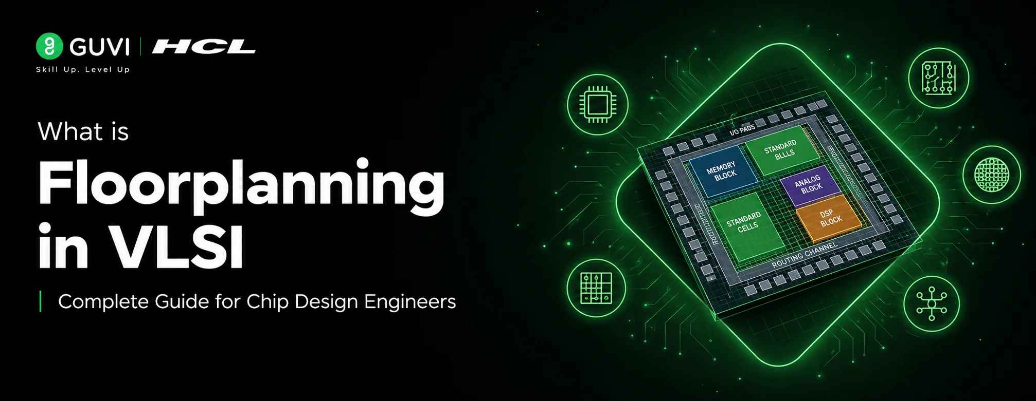
What is Floorplanning in VLSI: Complete Guide for Chip Design Engineers
Aug 03, 2026 7 Min Read 310 Views
(Last Updated)
Table of contents
- TL;DR Summary
- Introduction
- Understanding Floorplanning in VLSI
- Definition of Floorplanning in VLSI
- Objectives of Floorplanning in VLSI
- Evolution of Floorplanning Techniques
- Why Floorplanning Matters?
- Deep Dive into the Physical Design Flow
- Pre-Floorplanning Activities
- Floorplanning Phase Breakdown
- Post-Floorplanning Integration
- Advanced Floorplanning in VLSI Algorithms and Methodologies
- Spectral Partitioning
- Multilevel Partitioning
- Network Flow Methods
- Placement Optimization Techniques
- Simulated Annealing
- Force-Directed Placement
- Analytical Placement
- Critical Floorplanning in VLSI Constraints and Considerations
- Timing Constraints
- Power Constraints
- Manufacturing Constraints
- Key Components of a Chip Floorplan
- Hard Macros
- Soft Macros
- Standard Cells
- I/O Pads
- Floorplanning at Advanced Process Nodes
- Challenges at 3nm and 2nm Nodes
- Floorplanning in VLSI Design-for-Manufacturing Considerations
- Lithography-Aware Planning
- Yield Optimization
- Floorplanning in VLSI: Metrics and Evaluation Criteria
- Area Utilization Metrics
- Performance Metrics
- Routability Metrics
- Power Metrics
- Best Practices for Effective Floorplanning in VLSI
- Comparison Table: Good vs Poor Floorplanning
- Real-World Example: Smartphone Processor Design
- Common Mistakes in VLSI Floorplanning
- Advance Your VLSI Skills with HCL GUVI
- Conclusion
- Frequently Asked Questions
- What is the difference between floorplanning in VLSI and placement in VLSI?
- How long does the floorplanning phase typically take?
- What tools are commonly used for VLSI floorplanning?
- Can floorplanning affect power consumption?
- Is floorplanning automated or manual?
- What happens if floorplanning is done poorly?
- What skills are essential for VLSI floorplanning engineers in 2026?
- How is AI transforming floorplanning in 2026?
- What are the biggest challenges in floorplanning at 3nm and below?
- How do you evaluate floorplanning quality before moving to placement?
TL;DR Summary
- Floorplanning in VLSI is the foundational stage of physical design where engineers determine the optimal placement of functional blocks, memory arrays, and I/O pads on a chip.
- It directly impacts performance, power consumption, and area utilization.
- Done correctly, it sets the stage for successful routing, timing closure, and manufacturing yield.
- Poor floorplanning leads to congested layouts, timing violations, and increased costs.
Introduction
In today’s high-performance computing landscape, where chips power everything from smartphones to data centers, effective floorplanning determines whether a design meets its performance targets while staying within power and area budgets.
But what exactly is floorplanning in VLSI, and why does it carry such weight in the semiconductor industry?
With the global semiconductor market projected to reach $975 billion in annual sales in 2026, and the VLSI semiconductor market expected to grow at a CAGR of 6.7% from 2026 to 2034, mastering floorplanning becomes critical for career advancement in this expanding industry.
This comprehensive guide will walk you through the essentials of floorplanning in VLSI, helping you understand its role in the broader physical design flow and how to execute it effectively.
Understanding Floorplanning in VLSI
Definition of Floorplanning in VLSI
Floorplanning in VLSI is the initial phase of physical design where designers determine the physical arrangement of functional blocks, memory arrays, I/O pads, and other components on a silicon die.
Think of it as creating a strategic map that defines where each piece of the puzzle will go before assembly begins.
Objectives of Floorplanning in VLSI
The primary objectives of floorplanning include:
- Optimizing area utilization to minimize chip size and cost
- Establishing timing-critical block proximities to reduce signal delays
- Planning power distribution networks for stable operation
- Pre-planning routing channels to avoid congestion
- Ensuring manufacturability through design rule compliance
If you’re just beginning your VLSI journey, explore our complete guide on “How to Start a Career in VLSI” to understand career paths, required skills, and industry opportunities.
Evolution of Floorplanning Techniques
Traditional floorplanning relied heavily on manual placement by experienced engineers. However, as chip complexity increased exponentially, automated approaches became essential. Modern floorplanning combines:
- Algorithmic Approaches: Mathematical optimization techniques to solve placement problems
- Machine Learning Integration: AI-driven predictions for congestion and timing analysis
- Hierarchical Planning: Breaking complex designs into manageable sub-blocks
- Constraint-Driven Optimization: Balancing multiple competing objectives simultaneously
The Electronic Design Automation (EDA) tools market, which includes floorplanning software, is estimated at $20.78 billion in 2026, reflecting the industry’s heavy reliance on sophisticated tools for this critical process.
Why Floorplanning Matters?
The quality of floorplanning directly correlates with final chip performance. Timing closure issues can be traced back to poor floorplanning decisions. Additionally, well-executed floorplanning can reduce routing congestion, leading to more predictable design closure timelines.
Poor floorplanning, on the other hand, often results in:
- Increased wire lengths causing higher delay
- Routing bottlenecks that complicate backend processes
- Power delivery inefficiencies
- Higher electromagnetic interference
- Reduced manufacturing yield
With the semiconductor industry growing at an unprecedented pace, VLSI engineers who master floorplanning position themselves at the core of innovation.
Deep Dive into the Physical Design Flow
Pre-Floorplanning Activities
Before initiating the floorplanning phase, several preparatory steps must be completed:
- RTL Synthesis: Converting high-level behavioral descriptions to gate-level representations
- Technology Mapping: Adapting the design to the target fabrication process
- Constraint Collection: Gathering timing, power, and area specifications
- Library Characterization: Understanding cell behavior under various conditions
These activities provide the foundational data required for informed floorplanning decisions.
Floorplanning Phase Breakdown
1. Die Area Definition
The first step involves defining the total area available for the design:
- Setting chip dimensions based on packaging requirements
- Defining core area boundaries excluding periphery regions
- Planning for test structures and margin areas
2. Block Partitioning
Functional partitioning divides the design into logical blocks:
- Top-Down Approach: Starting with system-level partitions
- Bottom-Up Approach: Grouping related functions together
- Mixed Approach: Combining both strategies for optimal results
Modern partitioning techniques consider:
- Functional relationships between modules
- Timing requirements and critical paths
- Power domain boundaries
- Test accessibility requirements
3. Macro Placement
Placing large pre-designed blocks (memories, processors, analog IPs):
- Considering orientation and aspect ratio effects
- Planning surrounding routing channels
- Aligning with power grid structures
- Accounting for thermal characteristics
4. Pin Assignment
Defining connection points for inter-block communication:
- Optimizing for wirelength reduction
- Grouping related signals together
- Avoiding routing conflicts
- Meeting electrical requirements
5. Power Planning
Establishing power distribution infrastructure:
- Planning power ring dimensions
- Determining strap placement and widths
- Calculating IR drop requirements
- Planning for multiple voltage domains
Post-Floorplanning Integration
After completing the floorplanning phase, several activities ensure a smooth transition to subsequent stages:
- Congestion Analysis: Evaluating routing demand versus available resources
- Timing Budgeting: Distributing timing slack among blocks
- Physical Verification: Checking initial design rule compliance
- Documentation: Recording placement and constraint information
Floorplanning is only one stage of physical design. If you’re planning a career in backend VLSI, explore our HCL GUVI VLSI Training guide to understand the complete design flow, tools, and industry expectations.
Advanced Floorplanning in VLSI Algorithms and Methodologies
Effective partitioning is fundamental to successful floorplanning. Key algorithms include:
Spectral Partitioning
This technique uses eigenvalues of graph Laplacians to find balanced partitions:
- Constructs a graph representation of the design
- Computes eigenvectors to identify natural cut points
- Balances partition sizes while minimizing interconnection
- Particularly effective for regular structures
Multilevel Partitioning
A hierarchical approach combining coarsening and refinement:
- Coarsening: Reducing problem size through successive clustering
- Initial Partitioning: Solving the simplified problem
- Uncoarsening: Projecting solution back to original size
- Local Optimization: Improving the projected solution
Network Flow Methods
Treating partitioning as a flow optimization problem:
- Models connections as network flows
- Uses minimum cut algorithms to find optimal partitions
- Balances computational complexity with solution quality
Placement Optimization Techniques
Once partitioning is complete, optimizing block locations becomes critical:
Simulated Annealing
A probabilistic optimization technique inspired by metallurgy:
- Starts with random placement
- Iteratively moves blocks to reduce cost function
- Accepts worse solutions with decreasing probability
- Effective for escaping local minima
Force-Directed Placement
Models blocks as physical entities with attractive/repulsive forces:
- Attractive forces between connected blocks
- Repulsive forces between all blocks
- Equilibrium position determines final placement
- Fast convergence but potential for local optima
Analytical Placement
Uses mathematical optimization to solve placement directly:
- Formulates placement as a quadratic assignment problem
- Employs linear programming relaxations
- Provides high-quality solutions but computationally intensive
- Often combined with other techniques for practical deployment
Curious how artificial intelligence is transforming chip design? Read our article on AI in the Semiconductor Industry to discover how machine learning is optimizing floorplanning, placement, verification, and EDA workflows.
Critical Floorplanning in VLSI Constraints and Considerations
Timing Constraints
Timing is perhaps the most critical constraint in floorplanning:
- Path Length Requirements: Ensuring critical signals meet timing budgets
- Clock Domain Proximity: Minimizing skew between related clock domains
- Buffer Insertion Sites: Planning for signal integrity improvements
- Repeater Placement: Managing long interconnect delays
Modern designs often require:
- Multiple timing modes (functional, test, standby)
- Voltage corner analysis (fast, slow, typical)
- Temperature variation considerations
- Process variation accommodation
Power Constraints
Power management has become increasingly complex:
- IR Drop Prevention: Ensuring adequate voltage delivery across the die
- Electromigration Avoidance: Limiting current densities in metal traces
- Power Domain Organization: Grouping blocks with similar power requirements
- Dynamic Power Management: Supporting power gating and voltage scaling
Advanced techniques include:
- Statistical power analysis for worst-case scenarios
- Thermal-aware placement to prevent hotspots
- Power mesh optimization for multiple supply voltages
- Ground bounce minimization for I/O intensive designs
Manufacturing Constraints
Physical realizability imposes numerous restrictions:
- Design Rule Checks: Geometry constraints from fabrication processes
- Density Requirements: Uniform pattern distribution for lithography
- Antenna Rules: Preventing charge accumulation during processing
- CMP Considerations: Chemical mechanical polishing uniformity
At advanced nodes, additional complexities arise:
- Double/triple patterning requirements
- EUV lithography limitations
- FinFET-specific layout constraints
- Variability-aware design considerations
Key Components of a Chip Floorplan
Hard Macros
Hard macros are pre-designed, fixed-layout blocks like memories, processors, or analog components. They cannot be modified during physical design and must be placed as rigid units. Examples include:
- SRAM blocks
- ROM arrays
- ADC/DAC converters
- IP cores from third parties
When placing hard macros, engineers must consider:
- Orientation and aspect ratio
- Surrounding routing channels
- Power delivery requirements
- Thermal characteristics
Soft Macros
Unlike hard macros, soft macros have flexible boundaries and can be reshaped during physical design. These typically represent logic blocks whose exact dimensions can be adjusted for optimal floorplan utilization.
Placement flexibility allows engineers to optimize for:
- Wirelength reduction
- Congestion avoidance
- Timing optimization
Standard Cells
Standard cells form the basic building blocks of digital logic – AND gates, OR gates, flip-flops, etc. During floorplanning, regions are allocated for these cells based on logical partitioning.
Key considerations include:
- Cell density requirements
- Power grid planning
- Clock domain boundaries
I/O Pads
Input/Output pads interface the chip with the external world.

Their placement requires careful consideration of:
- Package routing constraints
- ESD protection requirements
- Signal integrity concerns
- Test access needs
Floorplanning at Advanced Process Nodes
Challenges at 3nm and 2nm Nodes
As process geometries shrink, floorplanning becomes increasingly complex:
Physical Effects Amplification
- Variability Impact: Process variations have proportionally larger effect
- Quantum Effects: Tunneling currents become significant
- Thermal Density: Heat dissipation becomes more challenging
- Parasitic Sensitivity: Small geometry changes cause large electrical shifts
Design Complexity Increase
- Multi-Patterning Requirements: Coloring constraints affect placement
- EUV Lithography: Specific pattern requirements for exposure
- FinFET Structures: Discrete device placement considerations
- Advanced Packaging: Integration with 2.5D/3D stacking
Floorplanning in VLSI Design-for-Manufacturing Considerations
Modern floorplanning must account for manufacturing realities:
Lithography-Aware Planning
- Pattern Density Control: Ensuring uniform exposure across die
- Forbidden Pattern Avoidance: Eliminating lithography problem patterns
- Resolution Enhancement: Planning for OPC and RET application
- Edge Placement Error: Managing critical dimension variations
Yield Optimization
- Redundancy Planning: Including spare structures for repair
- Test Structure Integration: Facilitating manufacturing validation
- Process Window Maximization: Enhancing robustness to variations
- Defect Avoidance: Steering clear of high-defect-density regions
Floorplanning in VLSI: Metrics and Evaluation Criteria
Successful floorplanning can be measured through several quantitative metrics:
Area Utilization Metrics
- Core Utilization: Percentage of core area occupied by logic
- Macro Density: Concentration of large blocks in specific regions
- Whitespace Distribution: Uniformity of unused space across die
- Aspect Ratio Quality: Rectangularity of block shapes
Performance Metrics
- Estimated Wirelength: Total interconnection length prediction
- Timing Slack Distribution: Spread of timing margins across paths
- Clock Skew: Variation in clock arrival times
- Signal Integrity Margins: Noise immunity measures
Routability Metrics
- Congestion Maps: Visualization of routing resource demand
- Channel Density: Metal track usage per routing region
- Via Requirements: Vertical connection point distributions
- Preferred Direction Compliance: Alignment with metal layer orientations
Power Metrics
- IR Drop Estimates: Voltage variation across power distribution
- Electromigration Risk: Current density violation indicators
- Power Grid Robustness: Resistance to supply variations
- Thermal Hotspot Identification: Localized heating predictions
Best Practices for Effective Floorplanning in VLSI
Following established best practices can dramatically improve floorplanning outcomes:
- Early Constraint Capture: Gather all timing, power, and area constraints before beginning floorplanning
- Incremental Refinement: Start with coarse placement and gradually refine details
- Congestion Awareness: Continuously monitor routing demand during placement decisions
- Hierarchical Planning: Break complex designs into manageable sub-blocks
- Design Reuse: Leverage previously validated placements where applicable
- Collaborative Review: Involve backend teams early in the planning process
- Physical Verification Integration: Check design rules throughout the process
- Scenario Analysis: Evaluate multiple floorplan alternatives systematically
Comparison Table: Good vs Poor Floorplanning
| Aspect | Good Floorplanning | Poor Floorplanning |
| Block Placement | Logical grouping, minimized wirelength | Random placement, excessive crossing |
| Power Grid | Adequate straps, uniform distribution | Insufficient planning, IR drop issues |
| Routing | Predictable channels, low congestion | Bottlenecks, frequent violations |
| Timing | Proximity maintained for critical paths | Long interconnect delays |
| Sign-off | Smooth verification process | Multiple iterations required |
| Manufacturing | DFM rules compliance | Yield-limiting violations |
| Scalability | Accommodates design changes | Requires major restructuring |
At 3nm and below process nodes, floorplanning decisions can impact final chip performance by up to 30%, making this phase even more critical than in previous generations.
Real-World Example: Smartphone Processor Design
Consider the design of a modern application processor for smartphones. Such chips integrate:
- CPU clusters (high-performance and efficiency cores)
- GPU for graphics processing
- Neural processing units for AI tasks
- Modem for cellular connectivity
- Image signal processors
- Various memory controllers
Effective floorplanning ensures:
- CPU and GPU stay close for shared cache access
- Modem is isolated to prevent RF interference
- Power domains align with functional blocks
- Thermal hotspots are avoided through strategic placement
Companies like Qualcomm and MediaTek invest heavily in sophisticated floorplanning methodologies to achieve competitive performance-per-watt metrics in their flagship chips.
With the Indian VLSI industry exhibiting distinct patterns in job availability across different domains, understanding these real-world applications becomes crucial for career advancement.
Common Mistakes in VLSI Floorplanning
Even experienced engineers can fall into certain traps during floorplanning:
- Overlooking Physical Constraints: Ignoring package limitations or thermal requirements early in the process
- Insufficient Margin Planning: Underestimating routing resources needed for complex interconnections
- Neglecting Timing Proximity: Placing tightly coupled blocks too far apart, creating excessive delay
- Inadequate Power Planning: Failing to allocate sufficient space for power distribution networks
- Ignoring Manufacturability: Making placements that violate design rules or create lithography challenges
- Premature Optimization: Spending too much time on minor details instead of addressing major architecture
- Inadequate Documentation: Failing to record constraint rationale for future reference
Advance Your VLSI Skills with HCL GUVI
Ready to master advanced VLSI design techniques including floorplanning? Our comprehensive VLSI Design and Verification Course covers everything from RTL coding to physical design implementation.
As highlighted in our guide on how to start a career in VLSI, learning industry-standard tools and methodologies is crucial for success in this rapidly growing field.
Learn from industry experts with over 25 years of experience in VLSI design and gain hands-on experience with real-world projects.
Enroll today to join thousands of successful alumni working at top semiconductor companies worldwide. Our HCL GUVI for VLSI Training offers flexibility that traditional courses cannot match, making it ideal for both final-year students and working professionals.
Explore the VLSI Design Course
Conclusion
Floorplanning in VLSI represents much more than just block placement; it’s the strategic foundation upon which successful chip designs are built.
From determining optimal macro arrangements to establishing power distribution networks, floorplanning decisions echo through every subsequent stage of the physical design flow.
As chips become increasingly complex with billions of transistors and multiple specialized processing units, mastering floorplanning becomes ever more critical.
Engineers who understand both the technical aspects and strategic implications of floorplanning position themselves at the forefront of semiconductor innovation.
Frequently Asked Questions
1. What is the difference between floorplanning in VLSI and placement in VLSI?
Floorplanning focuses on high-level organization of functional blocks and major components on the chip, while placement deals with precise positioning of individual standard cells within those predefined regions. Floorplanning sets the strategic foundation, whereas placement executes the tactical details.
2. How long does the floorplanning phase typically take?
For complex ASIC designs, floorplanning can take 2-4 weeks, depending on design complexity and team experience. This investment pays dividends by reducing iterations in later stages.
3. What tools are commonly used for VLSI floorplanning?
Industry-standard tools include Cadence Innovus, Synopsys IC Compiler, and Mentor Graphics Calibre. Open-source alternatives like OpenROAD are gaining popularity for academic and startup applications.
4. Can floorplanning affect power consumption?
Yes, floorplanning significantly impacts power through wirelength minimization, power domain organization, and placement of high-power blocks away from sensitive analog circuits.
5. Is floorplanning automated or manual?
Modern floorplanning combines automation with expert guidance. While tools handle basic placement, human expertise remains essential for strategic decisions and constraint optimization. In 2026, AI-assisted optimization tools are becoming increasingly prevalent.
6. What happens if floorplanning is done poorly?
Poor floorplanning leads to routing congestion, timing violations, excessive power consumption, and potentially failed tape-outs requiring expensive respins.
7. What skills are essential for VLSI floorplanning engineers in 2026?
Essential skills include proficiency in EDA tools, understanding of physical design flows, knowledge of advanced process technologies, and awareness of AI-driven design methodologies.
8. How is AI transforming floorplanning in 2026?
AI is revolutionizing floorplanning by enabling predictive congestion analysis, automated block placement optimization, and intelligent power grid planning. Machine learning algorithms can now suggest optimal configurations based on historical design data.
9. What are the biggest challenges in floorplanning at 3nm and below?
Key challenges include multi-patterning constraints, increased variability sensitivity, thermal management complexities, and stricter design rule requirements. Traditional approaches often fail at these nodes, necessitating new algorithmic solutions.
10. How do you evaluate floorplanning quality before moving to placement?
Quality assessment involves analyzing congestion maps, timing estimates, power grid adequacy, and design rule compliance. Modern tools provide comprehensive metrics dashboards to guide decision-making during this critical phase.
Success Stories

About the Author
Hashmithaa
Hi, I’m Hashmithaa — a content writer with a love for words. Writing isn’t just what I do; it’s how I connect, communicate, and create meaning in a noisy digital world. And if my words help someone make a better decision, learn something new, or feel more confident, then I’ve done my job well.
View all posts by Hashmithaa
Connect with me @
















Did you enjoy this article?