


VLSI Design Articles
Why Chips Fail: A Basic Guide to Chip Defects and IC Failure Analysis
Fun Facts About the Semiconductor Industry
Why Are Semiconductor Chips Expensive? Manufacturing Cost Explained
Instruction Set Architecture: How ISA Shapes Modern Chip Design


Get In Touch For Details! Request More Information
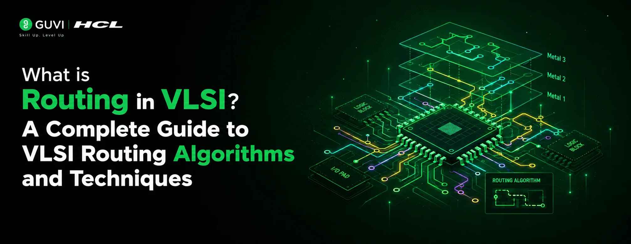
What is Routing in VLSI? A Complete Guide to VLSI Routing Algorithms and Techniques
Jul 31, 2026 8 Min Read 475 Views
(Last Updated)
Table of contents
- TL;DR
- Introduction
- What is Routing in VLSI?
- Why Routing Matters in VLSI Physical Design?
- Performance Impact
- Power Consumption
- Manufacturing Yield
- The Two Main Stages of VLSI Routing
- Global Routing Explained
- Detailed Routing Explained
- Comparison: Global Routing vs. Detailed Routing
- Key Routing Algorithms in VLSI
- Dijkstra's Algorithm
- A* Search Algorithm
- Lee's Maze Routing Algorithm
- Steiner Tree Routing
- Negotiated Congestion Routing (PathFinder Algorithm)
- Pattern-Based Routing
- Design Rules and Constraints in Routing
- Spacing Rules
- Width Rules
- Via Rules
- Layer Direction Rules
- Antenna Rules
- Electromigration Rules
- Challenges in Modern VLSI Routing
- Routing Congestion
- Design Rule Complexity
- Multi-Patterning Constraints
- Signal Integrity
- Power Delivery Network
- Routing Tools and EDA Software
- Cadence Innovus
- Synopsys ICC2
- Siemens Calibre
- Open-Source Tools
- Real-World Example: Routing in Smartphone Processors
- The Routing Process in Practice:
- Real-World Statistics:
- Common Mistakes to Avoid in VLSI Routing
- Mistake 1: Ignoring Congestion Analysis
- Mistake 2: Violating Design Rules
- Mistake 3: Poor Power Grid Planning
- Mistake 4: Neglecting Signal Integrity
- Mistake 5: Not Using Routing Constraints Effectively
- Ready to Master VLSI Routing?
- Conclusion
- Frequently Asked Questions
- What is routing in VLSI?
- What is the difference between global routing and detailed routing?
- Why is routing important in VLSI physical design?
- What algorithms are used in VLSI routing?
- What are the main challenges in VLSI routing?
- How long does the routing process take?
- What tools are used for VLSI routing?
- What are design rules in VLSI routing?
- Can routing affect chip timing?
- What is the relationship between placement and routing?
TL;DR
- Routing in VLSI is the process of creating electrical connections between logic components on an integrated circuit.
- It happens after placement and is divided into two main stages: global routing and detailed routing. Global routing plans the approximate path for wires, while detailed routing assigns exact wire segments to specific metal layers.
- This stage directly impacts chip performance, power consumption, and manufacturing yield.
- Modern routing algorithms handle billions of connections on advanced nodes such as 5nm and 3nm, making routing one of the most complex steps in physical design.
Introduction
When you design a modern microchip, you’re essentially building a city at the microscopic level. Just like a city needs roads to connect buildings, a chip needs wires to connect transistors, logic gates, and memory blocks. This connection process is called routing in VLSI.
Routing occurs after placement in the VLSI design flow. Placement decides where each component goes, and routing determines how they talk to each other. Without proper routing, even a perfectly placed chip won’t function.
The goal is simple: connect the right pins with the right wires while following strict design rules. But in practice, routing is one of the most computationally intensive steps in chip design.
You can think of VLSI routing as solving a massive 3D puzzle. The puzzle has millions of pieces, strict rules about where wires can go, and zero tolerance for mistakes.
What is Routing in VLSI?
Routing in VLSI is the process of creating electrical connections between logic components on an integrated circuit after placement determines where each element sits.
The process connects input and output pins using metal wires across multiple layers of the chip.
Modern processors require routing billions of connections across 12-15 metal layers, making it one of the most computationally intensive steps in physical design.
Why Routing Matters in VLSI Physical Design?
Routing directly affects three critical aspects of any integrated circuit: performance, power, and area.
Performance Impact
The length and routing path of a wire determine signal delay. Longer wires with poor routing increase resistance and capacitance, slowing down signals. In high-speed designs like server processors, even a few picoseconds matter.
Power Consumption
Poorly routed nets lead to higher parasitic capacitance. This increases dynamic power consumption. In battery-powered devices like smartphones, efficient routing can extend battery life significantly.
Manufacturing Yield
Routing must follow design rules to ensure the chip can be manufactured reliably. Violations like spacing errors or shorts can cause manufacturing defects, reducing yield and increasing cost.
Curious about how routing fits into India’s rapidly growing chip ecosystem? Explore India’s Semiconductor Mission to understand how the country is building a world-class semiconductor manufacturing and design industry.
A modern smartphone processor like the Apple A17 Pro contains over 11.7 billion transistors. Routing all these connections requires creating approximately 50-60 kilometers of wire interconnects compressed into a chip area smaller than 100 square millimeters. That’s equivalent to fitting the entire road network of a major city into a postage stamp!
The Two Main Stages of VLSI Routing
VLSI routing is performed in two distinct stages: global routing and detailed routing. Each stage has a specific purpose and uses different algorithms.
Global Routing Explained
Global routing is the first stage of the routing process. It divides the chip into a grid of routing regions called “global routing cells” or “gcells.”
The global router determines which gcells a net should pass through to connect its pins. It doesn’t specify exact wire positions or metal layers. Instead, it creates a high-level roadmap.
Key Functions of Global Routing:
- Plans approximate paths for all nets
- Balances routing congestion across the chip
- Assigns nets to routing regions
- Estimates wire lengths and delays
Global routing handles the “big picture” planning. Think of it as planning a road trip route on a map. You know which cities you’ll pass through, but not which specific streets.
Detailed Routing Explained
Detailed routing is the second and final stage. It takes the global routing solution and creates the actual wire segments.
The detailed router assigns each wire to a specific metal layer, track, and via position. It must follow all design rules while completing all connections.
Key Functions of Detailed Routing:
- Assigns exact wire positions on metal layers
- Places vias to connect different metal layers
- Fixes design rule violations
- Optimizes wire lengths and via counts
Detailed routing is like actually driving the route. You choose specific streets, lanes, and turns to reach your destination.
Comparison: Global Routing vs. Detailed Routing
| Aspect | Global Routing | Detailed Routing |
| Purpose | High-level path planning | Exact wire placement |
| Granularity | Routing regions (gcells) | Individual tracks and vias |
| Output | Approximate wire paths | Complete wire geometry |
| Complexity | Lower computational cost | Higher computational cost |
| Algorithms Used | Congestion-based, Steiner tree | Maze routing, A* search |
| Time Required | Hours | Hours to days |
| Design Rules | Not enforced | Fully enforced |
Key Routing Algorithms in VLSI
VLSI routing uses various algorithms to solve the routing problem efficiently. Here are the most important ones you should know.
1. Dijkstra’s Algorithm
Dijkstra’s algorithm is a shortest path algorithm developed by computer scientist Edsger W. Dijkstra in 1956. It finds the minimum-cost path between two points in a weighted graph.
How It Works in VLSI Routing:
- Treats each routing point as a node in a graph
- Edges represent possible wire segments with costs (wire length, congestion, layer penalty)
- Explores all paths from the source, always expanding the lowest-cost node first
- Guarantees finding the optimal shortest path
Advantages:
- Guarantees optimal solution
- Simple to implement and understand
- Works well for single-net routing
Limitations:
- Computationally expensive for large designs (O(n²) complexity)
- Explores many unnecessary paths
- Doesn’t scale well for millions of nets
Use Case: Dijkstra’s algorithm is used for routing critical timing paths where finding the absolute shortest path is essential, even at higher computational cost.
2. A* Search Algorithm
A* (pronounced “A-star”) is an informed search algorithm that improves upon Dijkstra’s approach. It was developed in 1968 by Peter Hart, Nils Nilsson, and Bertram Raphael.
How It Works:
A* uses a heuristic function to guide the search toward the destination:
f(n) = g(n) + h(n)
Where:
g(n) = actual cost from start to node n
h(n) = estimated cost from node n to destination (heuristic)
f(n) = total estimated path cost
Key Features:
- Uses Manhattan distance or Euclidean distance as heuristic
- Explores fewer nodes than Dijkstra while finding optimal paths
- Admissible heuristic guarantees optimality
Advantages:
- 50-100x faster than Dijkstra for typical routing problems
- Still finds optimal or near-optimal paths
- Widely used in commercial EDA tools
Use Case: A* is the most commonly used algorithm for detailed routing in modern EDA tools. It balances quality and speed effectively.
3. Lee’s Maze Routing Algorithm
Lee’s algorithm, developed by C.Y. Lee in 1961, is a breadth-first search (BFS) algorithm that treats routing as finding a path through a maze.
How It Works:
- Starts from the source pin and “floods” the routing grid
- Expands in all directions simultaneously (wave expansion)
- Labels each cell with its distance from the source
- Stops when reaching the target, then backtraces the path
Advantages:
- Guarantees finding the shortest path
- Can handle obstacles and blocked regions
- Works for any grid-based routing problem
Limitations:
- Very computationally expensive (O(n²) memory and time)
- Explores entire routing area regardless of destination
- Not practical for large-scale designs
Use Case: Lee’s algorithm is used for escape routing in PCB design and for small, complex routing problems where finding the shortest path is critical.
4. Steiner Tree Routing
Steiner tree algorithms solve the problem of connecting multiple pins with minimum total wire length. Unlike minimum spanning trees, Steiner trees can add intermediate points (Steiner points) to reduce total wire length.
How It Works:
- Given N pins, finds the shortest tree connecting all pins
- Can add Steiner points at any location to minimize total length
- The Rectilinear Steiner Tree (RST) is most common in VLSI (wires go horizontally/vertically)
Key Facts:
- For 3 pins, the optimal Steiner point is at the Fermat point
- Finding optimal Steiner trees is NP-hard for arbitrary pins
- Heuristic algorithms like FLUTE are used for practical designs
Advantages:
- Can reduce wire length by 10-15% compared to minimum spanning trees
- Reduces congestion by minimizing total wire usage
- Better timing due to shorter wire lengths
Use Case: Steiner tree routing is used in global routing to plan multi-pin net connections efficiently.
5. Negotiated Congestion Routing (PathFinder Algorithm)
Negotiated congestion routing is a modern approach developed specifically for FPGA and ASIC routing. The most famous implementation is the PathFinder algorithm by Betz and Rose (1997).
How It Works:
The algorithm works in iterations:
- Route all nets initially, ignoring congestion
- Identify conflicts where multiple nets use the same resource
- Increase cost of congested resources
- Reroute nets to avoid high-cost areas
- Repeat until all conflicts are resolved
Key Innovation:
- Instead of routing nets one-by-one, allows sharing initially
- Uses negotiation to resolve conflicts fairly
- Balances routing quality across all nets
Advantages:
- Handles high-congestion designs effectively
- Produces 10-20% better routing quality than sequential approaches
- Scales well to designs with millions of nets
Use Case: Negotiated congestion routing is used in modern FPGA tools (VPR, Vivado) and increasingly in ASIC routers for complex designs.
6. Pattern-Based Routing
Pattern-based routing uses predefined templates for common routing configurations instead of computing each route from scratch.
Common Patterns:
- L-shaped routing (two-segment connections)
- Z-shaped routing (three-segment connections)
- H-tree routing (for clock distribution)
Advantages:
- Very fast computation
- Predictable wire lengths
- Good for regular structures
Use Case: Pattern-based routing is used for clock tree routing, power grid routing, and regular datapath structures.
The routing problem in VLSI is NP-complete, meaning there’s no known algorithm that can always find the optimal solution efficiently. This was mathematically proven in 1977. For a chip with just 100 nets, the number of possible routing combinations exceeds the number of atoms in the observable universe (10^80). This is why modern routers use heuristics and approximation algorithms, running on powerful computing clusters for hours or days to find “good enough” solutions!

Design Rules and Constraints in Routing
VLSI routing must follow strict design rules to ensure manufacturability. Here are the key constraints routers must handle.
Spacing Rules
Wires on the same metal layer must maintain minimum spacing to avoid shorts. Different metal layers may have different spacing requirements.
Width Rules
Each metal layer has minimum and maximum wire width constraints. Width affects resistance and current-carrying capacity.
Via Rules
Vias connect wires on different metal layers. They must follow design rules for size, spacing, and enclosure.
Layer Direction Rules
Most processes assign preferred routing directions to each layer. For example, metal1 might route horizontally while metal2 routes vertically. This reduces routing conflicts.
Antenna Rules
During manufacturing, long metal wires can collect charge that damages transistor gates. Antenna rules limit wire lengths or require antenna diodes.
Electromigration Rules
Wires carrying high current must be wide enough to prevent electromigration failure. This is critical for power routing.
Challenges in Modern VLSI Routing
As technology nodes shrink to 7nm, 5nm, and 3nm, routing faces increasing challenges.
Routing Congestion
With billions of transistors on a chip, finding space for all wires becomes difficult. Congestion leads to detours, increasing delay and power.
Design Rule Complexity
Advanced nodes have hundreds of design rules. Routers must check and fix all violations while maintaining routability.
Multi-Patterning Constraints
Below 14nm, multi-patterning lithography adds complexity. Wires must be assigned to specific masks following strict rules.
Signal Integrity
Crosstalk between adjacent wires can cause timing violations and noise. Routers must minimize crosstalk through spacing and shielding.
Power Delivery Network
The power grid must deliver stable voltage across the chip. Power routing requires careful planning of widths and via arrays.
As chips become smaller and more complex, skilled VLSI engineers are in high demand. Discover how AI is transforming the Semiconductor Industry and reshaping chip design, verification, and physical design workflows.
The total wire length in a modern high-end processor exceeds 50 kilometers when laid end-to-end. Despite this enormous length, the entire routing is compressed into a chip area smaller than a fingernail. The wires are so thin that 1 kilometer of wire weighs less than 1 microgram. If you scaled up these wires to the thickness of a human hair, the chip would be the size of a football field!
Routing Tools and EDA Software
Several industry-standard EDA tools handle VLSI routing. Here are the most widely used ones.
Cadence Innovus
Cadence Innovus offers advanced routing capabilities for large, complex designs. Its “NanoRoute” engine handles global and detailed routing with sophisticated optimization.
Synopsys ICC2
Synopsys IC Compiler II (ICC2) provides comprehensive routing solutions. It includes advanced features for multi-patterning and signal integrity.
Siemens Calibre
While primarily a verification tool, Calibre works closely with routers to check and fix design rule violations.
Open-Source Tools
Tools like OpenROAD provide open-source routing solutions. These are valuable for learning and research purposes.
Real-World Example: Routing in Smartphone Processors
Let’s look at how routing works in a real product you use daily: your smartphone processor.
Modern smartphone chips like the Apple A17 Pro or Qualcomm Snapdragon 8 Gen 3 contain over 10 billion transistors. Routing all these connections requires sophisticated algorithms and massive computing power.
The Routing Process in Practice:
- Global Routing: The router divides the chip into routing regions, planning paths for billions of nets while managing congestion.
- Detailed Routing: Layer by layer, the router places actual wire segments. A chip like the A17 Pro uses 12-15 metal layers for routing.
- Optimization: The router iteratively improves wire lengths, via counts, and timing. This process can take several days on powerful servers.
- Verification: Design rule checks (DRC) verify all rules are met. Any violations are fixed before tape-out.
Real-World Statistics:
| Processor | Transistors | Metal Layers | Wire Length | Routing Time |
| Apple A17 Pro | 19 billion | 15 layers | ~60 km | 5-7 days |
| Snapdragon 8 Gen 3 | 16+ billion | 14 layers | ~55 km | 4-6 days |
| NVIDIA H100 | 80 billion | 18 layers | ~150 km | 10-14 days |
The result is a fully connected chip that delivers the performance you expect from your phone, all while fitting in a package smaller than your fingernail.
The routing problem in VLSI is NP-complete, meaning there’s no known algorithm that can always find the optimal solution efficiently. This is why modern routers use heuristics and approximation algorithms to find good solutions in reasonable time. For a chip with millions of nets, finding even a “good enough” routing solution requires sophisticated algorithms running on powerful computers for hours or days!
Common Mistakes to Avoid in VLSI Routing
Here are common mistakes that can cause routing failures or poor results.
Mistake 1: Ignoring Congestion Analysis
Skipping congestion analysis before routing leads to unroutable designs. Always analyze placement quality and congestion hotspots before detailed routing.
How to Avoid: Use global routing congestion maps to identify problems early. Adjust placement if necessary.
Mistake 2: Violating Design Rules
Even minor design rule violations can cause manufacturing failures. Routers sometimes create violations when pushing for better timing.
How to Avoid: Run thorough DRC checks after routing. Use router options that prioritize DRC cleanliness.
Mistake 3: Poor Power Grid Planning
Inadequate power routing causes voltage drops and electromigration problems. This can lead to chip failures in the field.
How to Avoid: Plan power grid early in the design flow. Use power analysis tools to verify adequate delivery.
Mistake 4: Neglecting Signal Integrity
Focusing only on connectivity while ignoring crosstalk leads to timing failures and noise issues.
How to Avoid: Enable signal integrity checks during routing. Add spacing and shielding where necessary.
Mistake 5: Not Using Routing Constraints Effectively
Failing to set proper routing constraints results in suboptimal timing and power.
How to Avoid: Define timing constraints, routing layers, and special net requirements before routing.
Ready to Master VLSI Routing?
Understanding routing in VLSI is essential for anyone pursuing a career in chip design.
If you want to learn these concepts hands-on and build real skills, check out the VLSI Design Course from HCL GUVI. This comprehensive program covers physical design, routing, routing algorithms, and industry-standard tools.
You’ll work on real projects and gain the practical knowledge that top semiconductor companies seek.
Conclusion
Modern routing algorithms handle billions of connections while following complex design rules. The quality of routing directly affects chip performance, power consumption, and manufacturing yield.
As technology advances to smaller nodes, routing challenges continue to grow, making it one of the most important skills for VLSI engineers. Understanding routing is essential for creating successful integrated circuits.
Frequently Asked Questions
1. What is routing in VLSI?
Routing in VLSI is the process of creating electrical connections between components on an integrated circuit. It occurs after placement and determines the exact paths wires take to connect pins while following design rules.
2. What is the difference between global routing and detailed routing?
Global routing plans approximate paths for nets across routing regions without specifying exact wire positions. Detailed routing assigns specific wire segments to metal layers and tracks, placing vias and ensuring all design rules are met.
3. Why is routing important in VLSI physical design?
Routing directly impacts chip performance through wire delays, power consumption through parasitic capacitance, and manufacturing yield through design rule compliance. Poor routing can cause chip failures or require costly respins.
4. What algorithms are used in VLSI routing?
Common routing algorithms include Dijkstra’s algorithm, A* search, Lee’s maze routing, Steiner tree algorithms, and negotiated congestion routing. Modern routers often combine multiple algorithms for optimal results.
5. What are the main challenges in VLSI routing?
Key challenges include routing congestion in dense designs, complex design rules in advanced nodes, signal integrity issues like crosstalk, power delivery network design, and multi-patterning constraints.
6. How long does the routing process take?
Routing time varies from hours to days depending on design complexity. For advanced designs with billions of transistors, routing can take several days on powerful computing clusters.
7. What tools are used for VLSI routing?
Industry-standard routing tools include Cadence Innovus with NanoRoute, Synopsys IC Compiler II, and open-source tools like OpenROAD. These tools handle global and detailed routing with various optimization features.
8. What are design rules in VLSI routing?
Design rules specify manufacturing constraints including minimum wire spacing, width requirements, via specifications, layer directions, antenna rules, and electromigration limits. All routing must comply with these rules.
9. Can routing affect chip timing?
Yes, routing significantly affects timing. Wire length, layer assignment, and via count determine signal delay. Critical nets require careful routing to meet timing constraints.
10. What is the relationship between placement and routing?
Placement determines component positions, creating the foundation for routing. Good placement improves routability and reduces wire lengths. Poor placement causes congestion and makes routing difficult or impossible.
Success Stories

About the Author
Hashmithaa
Hi, I’m Hashmithaa — a content writer with a love for words. Writing isn’t just what I do; it’s how I connect, communicate, and create meaning in a noisy digital world. And if my words help someone make a better decision, learn something new, or feel more confident, then I’ve done my job well.
View all posts by Hashmithaa
Connect with me @













Did you enjoy this article?