


VLSI Design Articles
Why Chips Fail: A Basic Guide to Chip Defects and IC Failure Analysis
Fun Facts About the Semiconductor Industry
Why Are Semiconductor Chips Expensive? Manufacturing Cost Explained
Instruction Set Architecture: How ISA Shapes Modern Chip Design


Get In Touch For Details! Request More Information
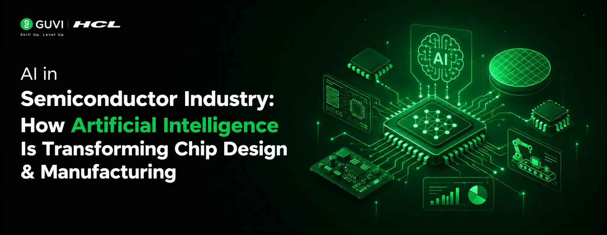
AI in Semiconductor Industry: How Artificial Intelligence Is Transforming Chip Design & Manufacturing
Jul 31, 2026 5 Min Read 517 Views
(Last Updated)
Table of contents
- TL;DR
- Introduction
- What is AI in Semiconductor Industry?
- Defining AI in Semiconductor Industry
- Key Components of AI in Semiconductor Industry
- Why It Matters
- How Is AI Used in Chip Design?
- AI Chip Design: The New Approach
- Placement and Routing Optimization
- Design Space Exploration
- Verification and Validation
- Machine Learning in VLSI: Applications & Benefits
- What is Machine Learning in VLSI?
- Key Applications of Machine Learning in VLSI
- Benefits Summary
- AI in Semiconductor Industry: Production & Quality
- The Manufacturing Challenge
- Defect Detection and Classification
- Predictive Maintenance
- Process Optimization
- Supply Chain Intelligence
- Real-World Examples of AI in Semiconductor Industry
- NVIDIA: AI-First Design Philosophy
- Intel: AI in Manufacturing
- TSMC: Yield Optimization Leader
- Google DeepMind: Floorplanning Breakthrough
- Comparison: Traditional vs AI-Powered Semiconductor Processes
- Common Mistakes to Avoid in AI Semiconductor Implementation
- Overestimating AI Capabilities
- Neglecting Data Quality
- Ignoring Human Expertise
- Underestimating Integration Challenges
- Focusing Only on Technology
- Career Opportunities in AI-Driven Semiconductor Industry
- Growing Demand
- Key Roles of AI-Driven Semiconductor Industry
- How to Get Started?
- Recommended Learning Path
- Conclusion
- FAQs
- What is AI in semiconductor industry?
- How is AI used in chip design?
- What is machine learning in VLSI?
- How does AI improve semiconductor manufacturing?
- Which companies use AI in semiconductor design?
- What are the benefits of AI in chip design?
- Can AI-designed chips be made without human intervention?
- What skills are needed for AI semiconductor careers?
- How is AI used in semiconductor testing?
TL;DR
- AI in semiconductor industry is reshaping how chips are designed, tested, and manufactured.
- From reducing design cycles by 30-50% to enabling defect detection with 99% accuracy, artificial intelligence is becoming indispensable.
- You’ll also learn about machine learning in VLSI and how AI in semiconductor manufacturing is driving efficiency. If you’re considering a career in this field, a VLSI Design Course can help you get started.
Introduction
The semiconductor industry powers everything from smartphones to self-driving cars. However, designing and manufacturing chips has become increasingly complex. With transistor counts exceeding 100 billion in modern processors, traditional methods alone cannot keep up.
This is where AI in semiconductor industry becomes a game-changer.
Artificial intelligence helps engineers design faster, detect defects earlier, and optimize manufacturing processes. Companies like NVIDIA, Intel, and TSMC are already using AI semiconductor technologies to stay competitive.
According to McKinsey, AI could create $1.6 trillion in annual value for the semiconductor industry by 2030. The technology reduces design time, improves yield rates, and enables innovations that were previously impossible.
If you’re an engineer or student looking to enter this field, understanding AI chip design and machine learning in VLSI is essential. Let’s explore how these technologies work and what they mean for the future.
What is AI in Semiconductor Industry?
Defining AI in Semiconductor Industry
AI in semiconductor industry refers to the application of artificial intelligence and machine learning technologies across the chip development lifecycle. This includes design, verification, testing, and manufacturing.
Unlike traditional rule-based systems, AI learns from data. It identifies patterns, predicts outcomes, and makes decisions with minimal human intervention.
Key Components of AI in Semiconductor Industry
| Component | Description |
| Machine Learning | Algorithms that learn from design data to optimize layouts and predict performance |
| Deep Learning | Neural networks for complex tasks like defect detection and pattern recognition |
| Computer Vision | Image analysis for wafer inspection and quality control |
| Generative AI | Creating new design options and optimizing existing architectures |
Why It Matters
The semiconductor industry faces three major challenges:
- Increasing complexity: Modern chips contain billions of transistors
- Rising costs: A new fab costs $10-20 billion
- Time-to-market pressure: Design cycles must shrink to stay competitive
AI semiconductor technologies address all three challenges simultaneously.
How Is AI Used in Chip Design?
AI Chip Design: The New Approach
Traditional chip design takes 18-24 months. Engineers manually create schematics, optimize layouts, and verify functionality. AI chip design changes this paradigm.
AI-powered tools can:
- Generate optimal layouts automatically based on specifications
- Predict performance before physical prototyping
- Identify design flaws early in the development cycle
- Optimize power consumption without sacrificing performance
Placement and Routing Optimization
One of the most time-consuming aspects of AI chip design is placement and routing. Engineers must position billions of components and connect them efficiently.
Google’s DeepMind developed an AI system that outperforms human experts in floorplanning. The system reduced design time from weeks to hours while improving power efficiency by 10-15%.
Design Space Exploration
AI enables rapid exploration of design alternatives. Instead of testing one configuration at a time, engineers can evaluate thousands of options simultaneously.
This approach leads to:
- Better performance-per-watt ratios
- Smaller die sizes
- Reduced manufacturing costs
Verification and Validation
Verification accounts for 50-70% of total design time. AI accelerates this process by:
- Automatically generating test cases
- Predicting potential failure modes
- Prioritizing critical verification paths
Machine Learning in VLSI: Applications & Benefits
What is Machine Learning in VLSI?
Machine learning in VLSI (Very Large Scale Integration) applies ML algorithms to design, test, and optimize integrated circuits. VLSI involves creating chips with thousands to billions of transistors.
Key Applications of Machine Learning in VLSI
1. Power Optimization
Power consumption is critical for mobile devices and data centers. Machine learning in VLSI helps engineers:
- Predict power usage at different workloads
- Optimize voltage and frequency dynamically
- Reduce leakage current through intelligent design
Example: Apple’s M-series chips use ML-based power management to deliver industry-leading battery life.
2. Timing Analysis
Timing violations cause chips to fail. ML algorithms can:
- Predict timing paths with 95% accuracy
- Identify critical paths before simulation
- Suggest optimizations automatically
3. Yield Prediction
Manufacturing yield affects profitability. Machine learning in VLSI enables:
- Early yield prediction based on design parameters
- Identification of yield-limiting factors
- Process optimization recommendations
4. Thermal Management
Overheating reduces performance and lifespan. ML models can:
- Predict thermal hotspots during design
- Optimize heat dissipation layouts
- Enable dynamic thermal management
Benefits Summary
| Benefit | Impact |
| Faster Time-to-Market | 30-50% reduction in design cycles |
| Lower Costs | 20-30% reduction in development costs |
| Higher Quality | 15-25% improvement in first-pass success |
| Better Performance | 10-15% improvement in power efficiency |
AI in Semiconductor Industry: Production & Quality
The Manufacturing Challenge
Semiconductor manufacturing involves 300-500 process steps. Each step must be precise to within nanometers. A single defect can render a chip useless.
AI in semiconductor manufacturing addresses these challenges through intelligent automation and predictive analytics.
Defect Detection and Classification
Traditional inspection systems miss subtle defects. AI-powered computer vision can:
- Detect defects invisible to human inspectors
- Classify defect types automatically
- Predict which defects will cause failures
Statistic: AI-based inspection systems achieve 99% defect detection accuracy compared to 85% for traditional methods.
Predictive Maintenance
Equipment failure costs fabs millions in downtime. AI in semiconductor manufacturing enables:
- Real-time equipment health monitoring
- Prediction of failures before they occur
- Optimized maintenance schedules
Process Optimization
Manufacturing processes must be continuously tuned. AI helps by:
- Adjusting parameters in real-time
- Compensating for equipment drift
- Optimizing yield across product lines
Supply Chain Intelligence
The semiconductor supply chain is complex and global. AI provides:
- Demand forecasting with 90% accuracy
- Inventory optimization
- Risk prediction and mitigation
AI in semiconductor manufacturing can detect defects as small as 10 nanometers. That’s roughly 10,000 times smaller than a human hair width. This precision is impossible with traditional inspection methods.
Real-World Examples of AI in Semiconductor Industry
NVIDIA: AI-First Design Philosophy
NVIDIA uses AI throughout its GPU design process. The company’s AI chip design approach includes:
- ML-optimized layouts for its H100 and A100 GPUs
- AI-powered verification reducing test time by 50%
- Predictive models for performance optimization
Result: NVIDIA reduced design cycles by 40% while delivering industry-leading performance.
Intel: AI in Manufacturing
Intel has deployed AI across its manufacturing facilities. Key applications include:
- AI-based defect detection at wafer inspection
- Predictive maintenance for fab equipment
- Process optimization using reinforcement learning
Statistic: Intel reported $100 million in annual savings from AI manufacturing optimization (2023).

TSMC: Yield Optimization Leader
TSMC uses AI in semiconductor manufacturing to maintain its yield advantage. Their approach includes:
- ML-based yield prediction models
- AI-driven process control
- Automated defect classification
Result: TSMC achieves 90%+ yield rates on advanced nodes, significantly higher than competitors.
Google DeepMind: Floorplanning Breakthrough
Google’s DeepMind developed an AI system that revolutionizes floorplanning. The system:
- Treats chip layout as a reinforcement learning problem
- Generates layouts in hours instead of weeks
- Outperforms human experts on key metrics
This breakthrough demonstrates how AI semiconductor technologies can surpass human capabilities.
Comparison: Traditional vs AI-Powered Semiconductor Processes
| Process | Traditional Approach | AI-Powered Approach | Improvement |
| Design Time | 18-24 months | 9-12 months | 50% faster |
| Layout Optimization | Manual, iterative | Automated, ML-driven | 10-15% better PPA |
| Verification | Rule-based, time-consuming | Intelligent, prioritized | 40% time reduction |
| Defect Detection | 85% accuracy | 99% accuracy | 14% improvement |
| Yield Prediction | Statistical methods | ML-based prediction | 25% more accurate |
| Maintenance | Scheduled/reactive | Predictive/proactive | 20% less downtime |
| Cost | High due to iterations | Lower due to first-pass success | 20-30% savings |
The first AI-designed chip was taped out in 2021. Google’s TPU v4 was designed using machine learning algorithms for floorplanning. This marked the first time AI created a production-ready chip layout, reducing design time from months to hours.
Common Mistakes to Avoid in AI Semiconductor Implementation
1. Overestimating AI Capabilities
AI is powerful but not magical. It requires quality data and proper training. Many companies expect AI to solve all problems immediately.
Solution: Start with well-defined use cases and realistic expectations.
2. Neglecting Data Quality
AI models are only as good as their training data. Poor data leads to poor predictions.
Solution: Invest in data infrastructure before AI implementation.
3. Ignoring Human Expertise
AI should augment, not replace, human engineers. Domain knowledge remains essential.
Solution: Combine AI tools with experienced engineers for best results.
4. Underestimating Integration Challenges
Integrating AI into existing workflows is complex. Many implementations fail due to poor integration.
Solution: Plan integration carefully and involve all stakeholders.
5. Focusing Only on Technology
Success requires more than technology. Process changes and skill development are equally important.
Solution: Develop a comprehensive implementation strategy including training and change management.
Career Opportunities in AI-Driven Semiconductor Industry
Growing Demand
The integration of AI in the semiconductor industry is creating new career opportunities. Companies need engineers who understand both semiconductor design and AI technologies.
Statistic: The global AI semiconductor market is expected to reach US $2 trillion by 2036.
Key Roles of AI-Driven Semiconductor Industry
| Role | Required Skills | Average Salary (India) |
| AI Chip Design Engineer | VLSI, ML, Python | ₹15-25 LPA |
| ML Engineer – Semiconductors | ML, Deep Learning, Hardware | ₹12-22 LPA |
| Design Verification Engineer | Verification, AI Tools | ₹10-20 LPA |
| Process Engineer – AI/ML | Manufacturing, Data Science | ₹8-18 LPA |
| AI Infrastructure Engineer | Hardware, AI Systems | ₹12-25 LPA |
How to Get Started?
If you want to build a career in this field, you need:
- Strong fundamentals in VLSI design and semiconductor physics
- AI/ML knowledge including neural networks and deep learning
- Programming skills in Python, Verilog, and C++
- Hands-on experience with industry tools
A structured learning program can help you acquire these skills efficiently.
Recommended Learning Path
The VLSI Design Course from HCL GUVI provides comprehensive training in:
- VLSI design fundamentals
- Digital and analog circuit design
- Verification methodologies
- Industry-standard tools
This course prepares you for roles in AI-driven semiconductor companies and helps you build practical skills through hands-on projects.
Conclusion
The AI in semiconductor industry represents one of the most significant technological shifts in recent decades. From AI chip design to manufacturing optimization, artificial intelligence is transforming every aspect of chip development.
Companies that embrace AI semiconductor technologies gain competitive advantages through faster design cycles, higher yields, and lower costs. Engineers who understand machine learning in VLSI and AI in semiconductor manufacturing will be in high demand.
The future of semiconductors is intelligent. By understanding and adopting these technologies today, you position yourself for success tomorrow.
FAQs
1. What is AI in semiconductor industry?
AI in semiconductor industry refers to using artificial intelligence and machine learning technologies across chip design, verification, testing, and manufacturing processes to improve efficiency, quality, and speed.
2. How is AI used in chip design?
AI in chip design automates layout optimization, accelerates verification, predicts performance, and enables design space exploration. It can reduce design time by 30-50% while improving power and performance metrics.
3. What is machine learning in VLSI?
Machine learning in VLSI applies ML algorithms to optimize integrated circuit design, including power management, timing analysis, yield prediction, and thermal management for chips with billions of transistors.
4. How does AI improve semiconductor manufacturing?
AI in semiconductor manufacturing enables defect detection with 99% accuracy, predictive maintenance to reduce downtime, process optimization for higher yields, and supply chain intelligence for better planning.
5. Which companies use AI in semiconductor design?
Major companies using AI semiconductor technologies include NVIDIA, Intel, TSMC, Google DeepMind, Samsung, and Qualcomm. These companies use AI for design, verification, and manufacturing optimization.
6. What are the benefits of AI in chip design?
Benefits include 50% faster design cycles, 20-30% cost reduction, 15-25% improvement in first-pass success rates, and 10-15% better power-performance-area metrics compared to traditional approaches.
7. Can AI-designed chips be made without human intervention?
AI can assist with specific tasks like floorplanning and optimization, but human expertise remains essential. The most effective approach combines AI tools with experienced engineers for optimal results.
8. What skills are needed for AI semiconductor careers?
Key skills include VLSI design fundamentals, machine learning and deep learning knowledge, programming in Python and Verilog, familiarity with industry tools, and understanding of semiconductor physics.
9. How is AI used in semiconductor testing?
AI improves semiconductor testing through intelligent test case generation, predictive failure analysis, automated defect classification, and optimization of test sequences to reduce time while maintaining coverage.
Success Stories

About the Author
Hashmithaa
Hi, I’m Hashmithaa — a content writer with a love for words. Writing isn’t just what I do; it’s how I connect, communicate, and create meaning in a noisy digital world. And if my words help someone make a better decision, learn something new, or feel more confident, then I’ve done my job well.
View all posts by Hashmithaa
Connect with me @














Did you enjoy this article?