Advance your semiconductor career with the CEP, IIT Delhi’s Digital VLSI Design certificate programme and build hands-on skills in RTL-to-GDSII design, verification, advanced chip implementation, and more. Perfect for beginners and working professionals alike!
Best Suited for:
Working professionals, Graduates aspiring to build a career in VLSI, and job seekers
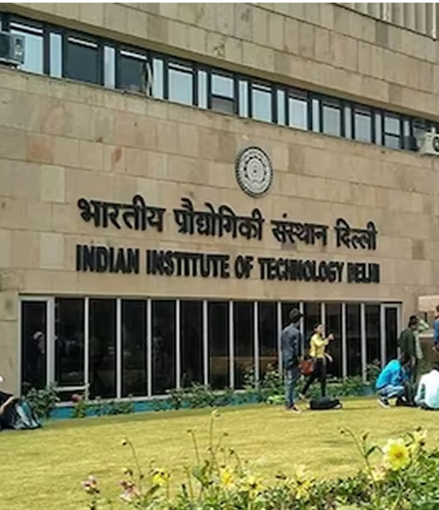
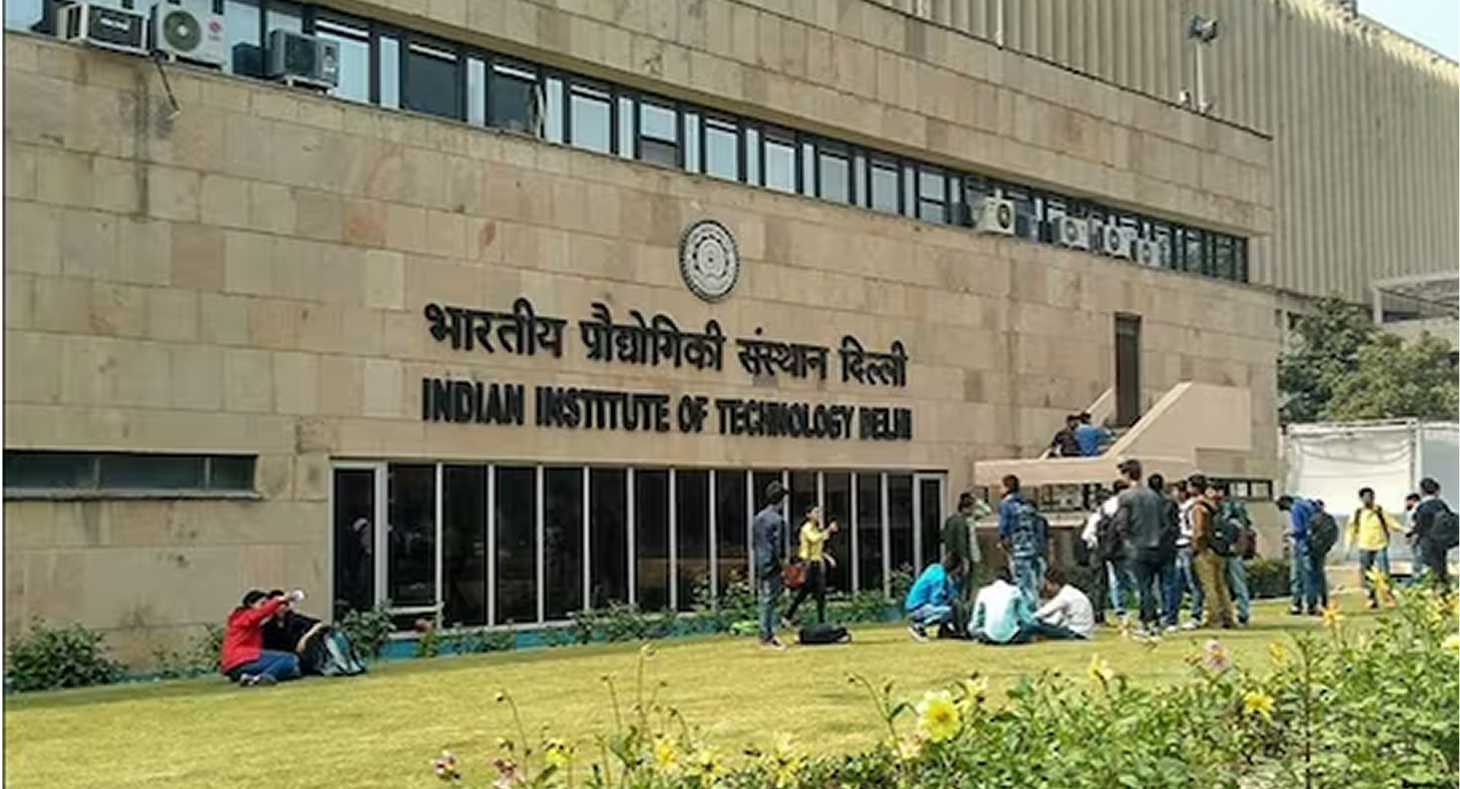
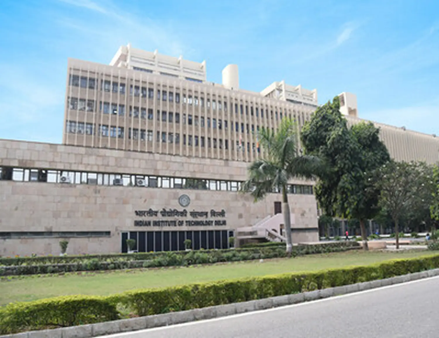
IIT Delhi ranked #1 in QS World University Rankings: India 2026
IIT Delhi ranked #2 in NIRF 2025 under the Engineering Category
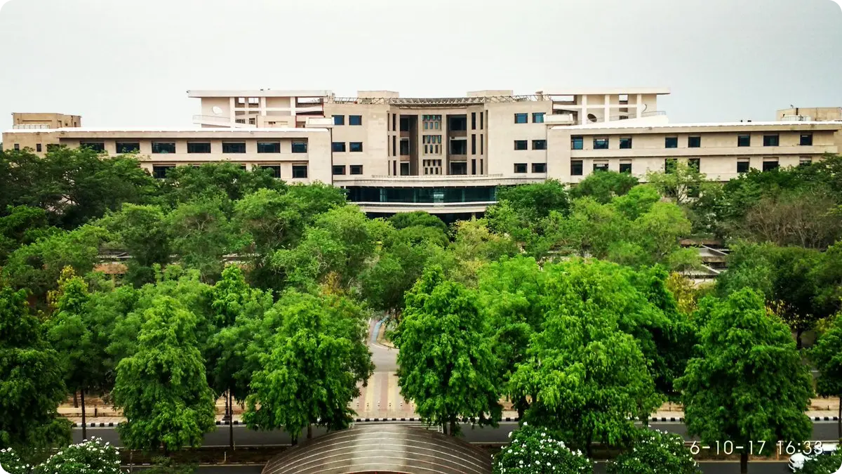
Campus Immersion at IIT Delhi *
Group Project & Peer-to-peer Learning
Guidance Directly from IIT Delhi Faculty
e-certification from IIT Delhi, CEP
*Travel and accommodation cost will be borne by the participants. IIT Delhi is not responsible for the same.
This structured curriculum guides you through CMOS design, RTL development, synthesis, verification, physical design, and low-power methodologies, covering the complete RTL to GDSII journey.
Eligibility Criteria
Candidates from Electronics, Electrical, Physics, Computer Science, or related backgrounds from a recognised university or institution are eligible.
Suitable for working professionals, graduates aspiring to build a career in VLSI, and job seekers.
Fresh graduates with an interest in semiconductor and VLSI technologies can also apply.
Admission Criteria
Executive education helps companies build a culture that embraces new technologies and adapts to changing business and regulatory needs.
IIT Delhi has launched Online Certificate Programmes under eVIDYA@IITD (ई-विद्या@IITD) – enabling Virtual & Interactive-learning for Driving Youth Advancement.
Programmes are accessible to both Indian and international participants.
Designed to meet the training and development needs of organisations, industries, society, and individuals at national and global levels.
Aims to empower learners with high-quality online education in engineering, technology, science, humanities, and management.
Focus on cutting-edge domains to support career growth and advancement.
CEP is the statutory body of IIT Delhi responsible for offering certificate programmes and issuing certificates.
To know more about CEP,IIT Delhi, visit: http://cepqip.iitd.ac.in/
This programme builds deep technical capability across the complete digital VLSI design lifecycle, combining theory, tool-based learning, and hands-on implementation experience.
Module 1
CMOS ASIC Design Flow
MOS Device Physics
CMOS Inverter
Combinational and Sequential Logic Gates
Module 5
Floor planning, Placement and Routing
CTS and Power Planning
Advanced Node Challenges: FinFET, EUV Lithography, Double Patterning
Module 2
Introduction to Linux
Scripting VLSI
VLSI Design Flow
RTL Coding and Design Styles
Module 6
Low Power Design Methodologies
Sources of Power Dissipation
UPF/CPF for Power-Aware Design
Module 3
Logic Synthesis Concepts and Optimization
Static Timing Analysis and Timing Concepts
Power-Aware Synthesis
Module 7
Introduction to Analog IC Design
PLL & Clock Generation Circuits
Mixed Signal Design
Module 4
Scan Chain Insertion, ATPG & BIST
Fault Models and Fault Coverage Metrices
Soft Errors, Reliability & Resilience in Nano-Scale VLSI
Module 8
Scan Chain Insertion, ATPG & BIST
Fault Models and Fault Coverage Metrices
Soft Errors, Reliability & Resilience in Nano-Scale VLSI
Projects
Learners apply theoretical concepts to real-world VLSI design challenges, developing practical skills, EDA tool proficiency, and industry-ready problem-solving capability.
Advance your semiconductor career with the CEP, IIT Delhi’s Digital VLSI Design certificate programme and build hands-on skills in RTL-to-GDSII design, verification, advanced chip implementation, and more. Perfect for beginners and working professionals alike!
Best Suited for:
Working professionals, Graduates aspiring to build a career in VLSI, and job seekers
IIT Delhi ranked #1 in QS World University Rankings: India 2026
IIT Delhi ranked #2 in NIRF 2025 under the Engineering Category
Campus Immersion at IIT Delhi *
Group Project & Peer-to-peer Learning
Guidance Directly from IIT Delhi Faculty
e-certification from IIT Delhi, CEP
*Travel and accommodation cost will be borne by the participants. IIT Delhi is not responsible for the same.
This structured curriculum guides you through CMOS design, RTL development, synthesis, verification, physical design, and low-power methodologies, covering the complete RTL to GDSII journey.
Eligibility Criteria
Candidates from Electronics, Electrical, Physics, Computer Science, or related backgrounds from a recognised university or institution are eligible.
Suitable for working professionals, graduates aspiring to build a career in VLSI, and job seekers.
Fresh graduates with an interest in semiconductor and VLSI technologies can also apply.
Admission Criteria
Executive education helps companies build a culture that embraces new technologies and adapts to changing business and regulatory needs.
IIT Delhi has launched Online Certificate Programmes under eVIDYA@IITD (ई-विद्या@IITD) – enabling Virtual & Interactive-learning for Driving Youth Advancement.
Programmes are accessible to both Indian and international participants.
Designed to meet the training and development needs of organisations, industries, society, and individuals at national and global levels.
Aims to empower learners with high-quality online education in engineering, technology, science, humanities, and management.
Focus on cutting-edge domains to support career growth and advancement.
CEP is the statutory body of IIT Delhi responsible for offering certificate programmes and issuing certificates.
To know more about CEP,IIT Delhi, visit: http://cepqip.iitd.ac.in/
This programme builds deep technical capability across the complete digital VLSI design lifecycle, combining theory, tool-based learning, and hands-on implementation experience.
Module 1
CMOS ASIC Design Flow
MOS Device Physics
CMOS Inverter
Combinational and Sequential Logic Gates
Module 2
Introduction to Linux
Scripting VLSI
VLSI Design Flow
RTL Coding and Design Styles
Module 3
Logic Synthesis Concepts and Optimization
Static Timing Analysis and Timing Concepts
Power-Aware Synthesis
Module 4
Scan Chain Insertion, ATPG & BIST
Fault Models and Fault Coverage Metrices
Soft Errors, Reliability & Resilience in Nano-Scale VLSI
Module 5
Floor planning, Placement and Routing
CTS and Power Planning
Advanced Node Challenges: FinFET, EUV Lithography, Double Patterning
Module 6
Low Power Design Methodologies
Sources of Power Dissipation
UPF/CPF for Power-Aware Design
Module 7
Introduction to Analog IC Design
PLL & Clock Generation Circuits
Mixed Signal Design
Module 8
Scan Chain Insertion, ATPG & BIST
Fault Models and Fault Coverage Metrices
Soft Errors, Reliability & Resilience in Nano-Scale VLSI
Projects
Learners apply theoretical concepts to real-world VLSI design challenges, developing practical skills, EDA tool proficiency, and industry-ready problem-solving capability.
Step 1
Select the Certificate Programme in Digital VLSI Design and complete your registration.
Step 2
Connect with our Programme Advisors for guidance and submit the application fee to move forward.
Step 3
Get your documents verified and appear for an interview if required.
Step 4
Receive your Offer Letter from the CEP, IIT Delhi and confirm your acceptance.
Step 5
Pay the programme fees to secure your seat.
Step 6
Complete onboarding and begin your learning journey in the Digital VLSI Design Programme.
Aspiring VLSI Professionals
Individuals looking to build a strong foundation in digital VLSI design and enter the rapidly growing semiconductor industry.
Working Engineers & Technologists
Professionals seeking to upskill in chip design, synthesis, physical implementation, and low-power methodologies to transition into semiconductor-focused roles.
Electronics, Electrical & CS Graduates
Graduates and diploma holders aiming to develop industry-relevant VLSI expertise and pursue careers in RTL to GDSII design domains.
Dr. Seema Sharma, head of the Department of Management Studies at IIT Delhi, specializes in Economics and Entrepreneurship, with research published in leading international journals.
She teaches Business Economics, Macroeconomic Environment, and Data Analysis to MBA and PhD students.
Dr. Sharma has presented globally and received awards like the ‘Outstanding Young Faculty Fellowship Award’ from IIT Delhi and the ‘Best Professor in Economics Award’ by Hindustan Unilever-BSA-Dewang Mehta Business School.
Dr. Gourav Dwivedi, an Assistant Professor in the Department of Management Studies at IIT Delhi, focuses on Operations and Supply Chain Management.
With over a decade of experience in both academia and industry, Dr. Dwivedi has contributed to various engineering service projects, particularly for Fortune 500 companies.
In academia, he has participated in collaborative research and consulting projects with national and international organizations, resulting in publications in leading journals. His research interests include Distributed Manufacturing, Supply Chain, Logistics Modelling, Industry 4.0, Behavioral Operations, Business Sustainability, and Systems Thinking.
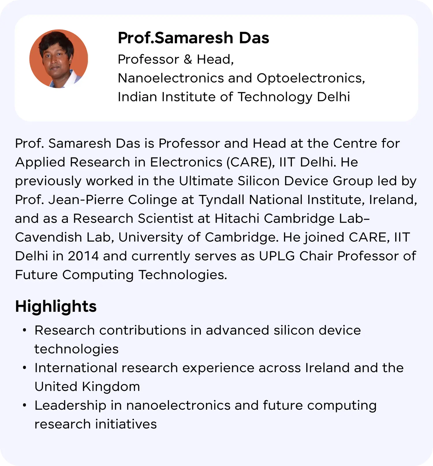
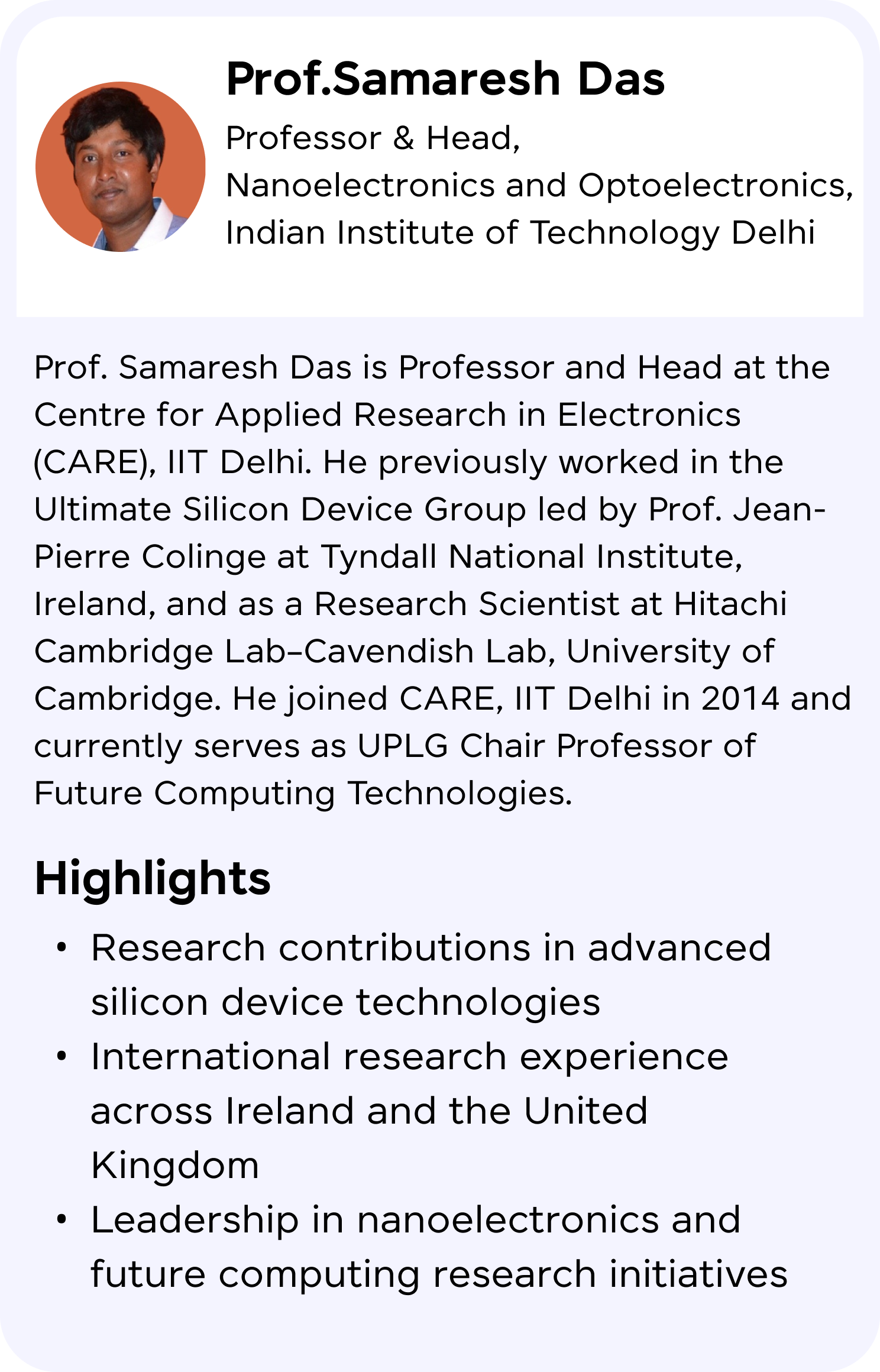
Professor & Head,
Nanoelectronics and Optoelectronics,
Indian Institute of Technology Delhi
Prof. Samaresh Das is Professor and Head at the Centre for Applied Research in Electronics (CARE), IIT Delhi. He previously worked in the Ultimate Silicon Device Group led by Prof. Jean-Pierre Colinge at Tyndall National Institute, Ireland, and as a Research Scientist at Hitachi Cambridge Lab–Cavendish Lab, University of Cambridge. He joined CARE, IIT Delhi in 2014 and currently serves as UPLG Chair Professor of Future Computing Technologies.
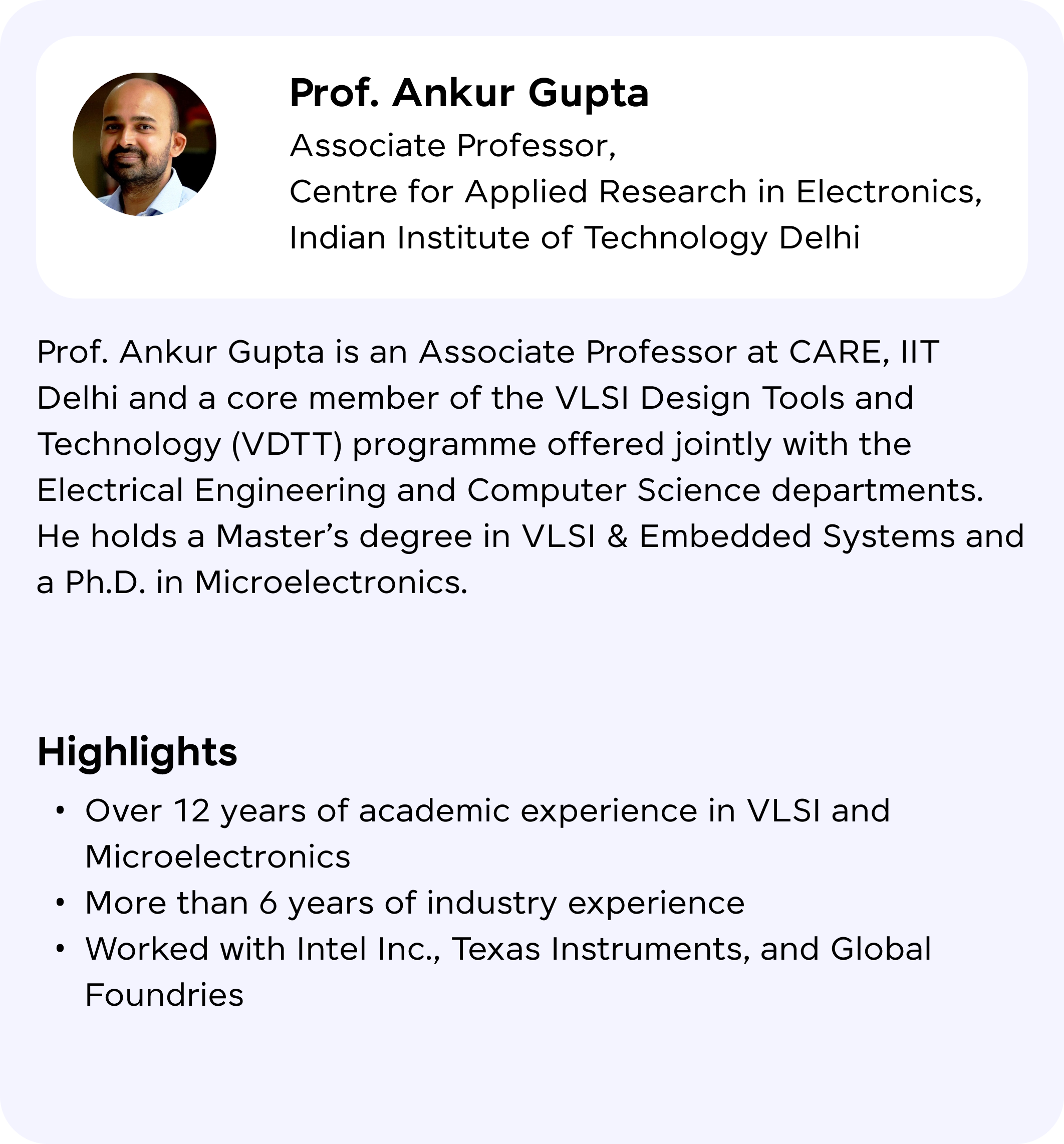
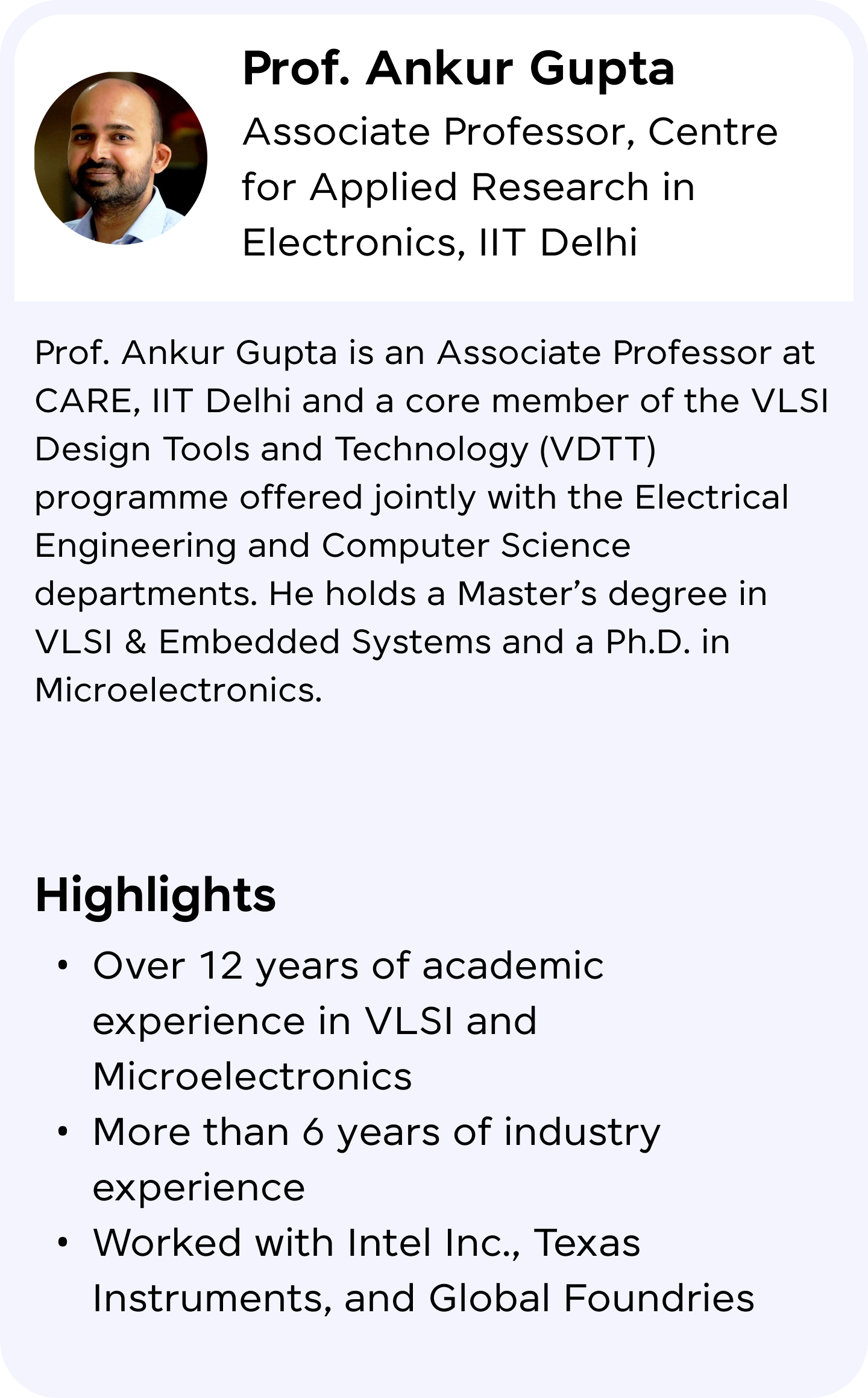
Associate Professor,
Centre for Applied Research in Electronics,
Indian Institute of Technology Delhi
Prof. Ankur Gupta is an Associate Professor at CARE, IIT Delhi and a core member of the VLSI Design Tools and Technology (VDTT) programme offered jointly with the Electrical Engineering and Computer Science departments. He holds a Master’s degree in VLSI & Embedded Systems and a Ph.D. in Microelectronics.
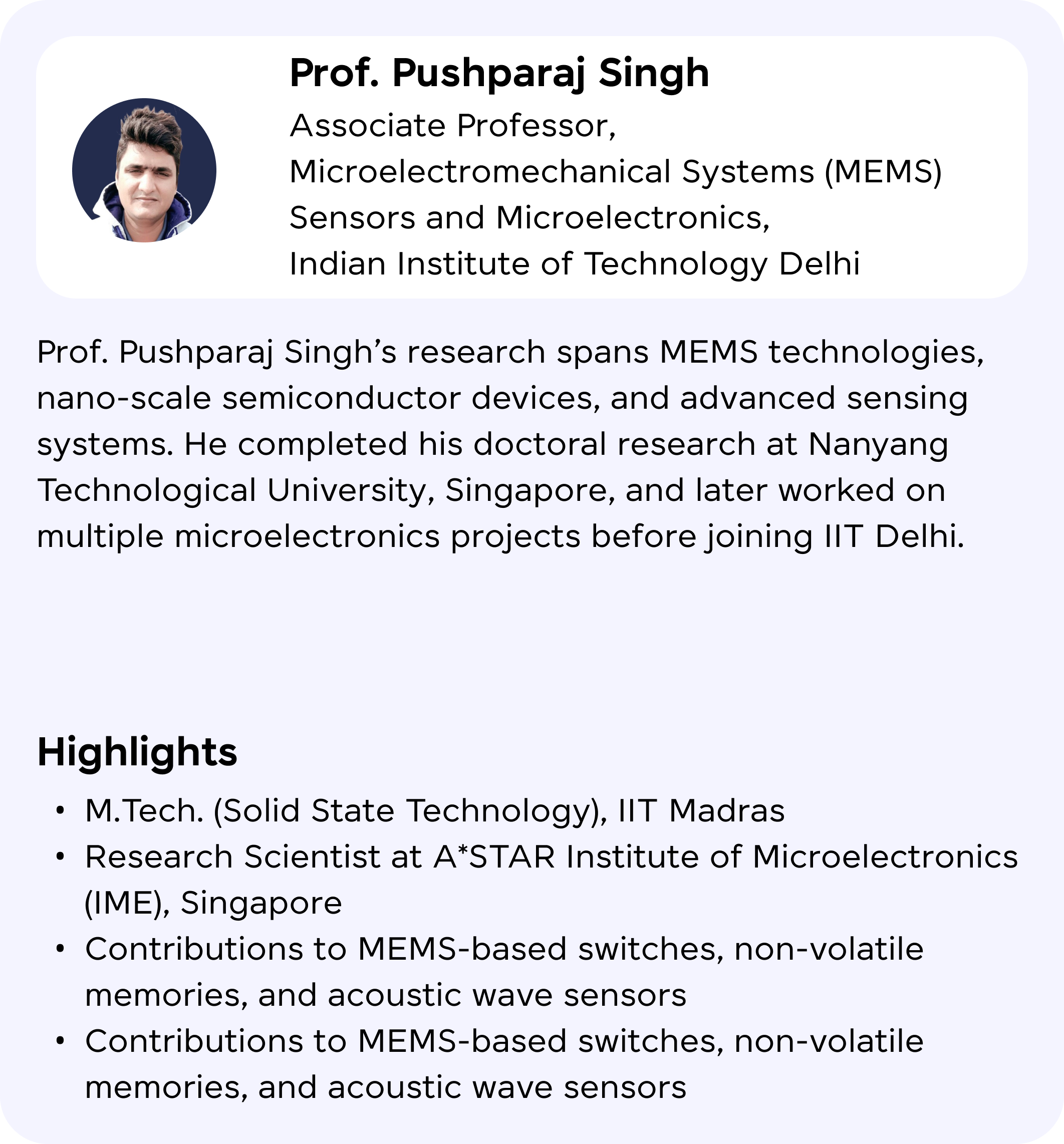
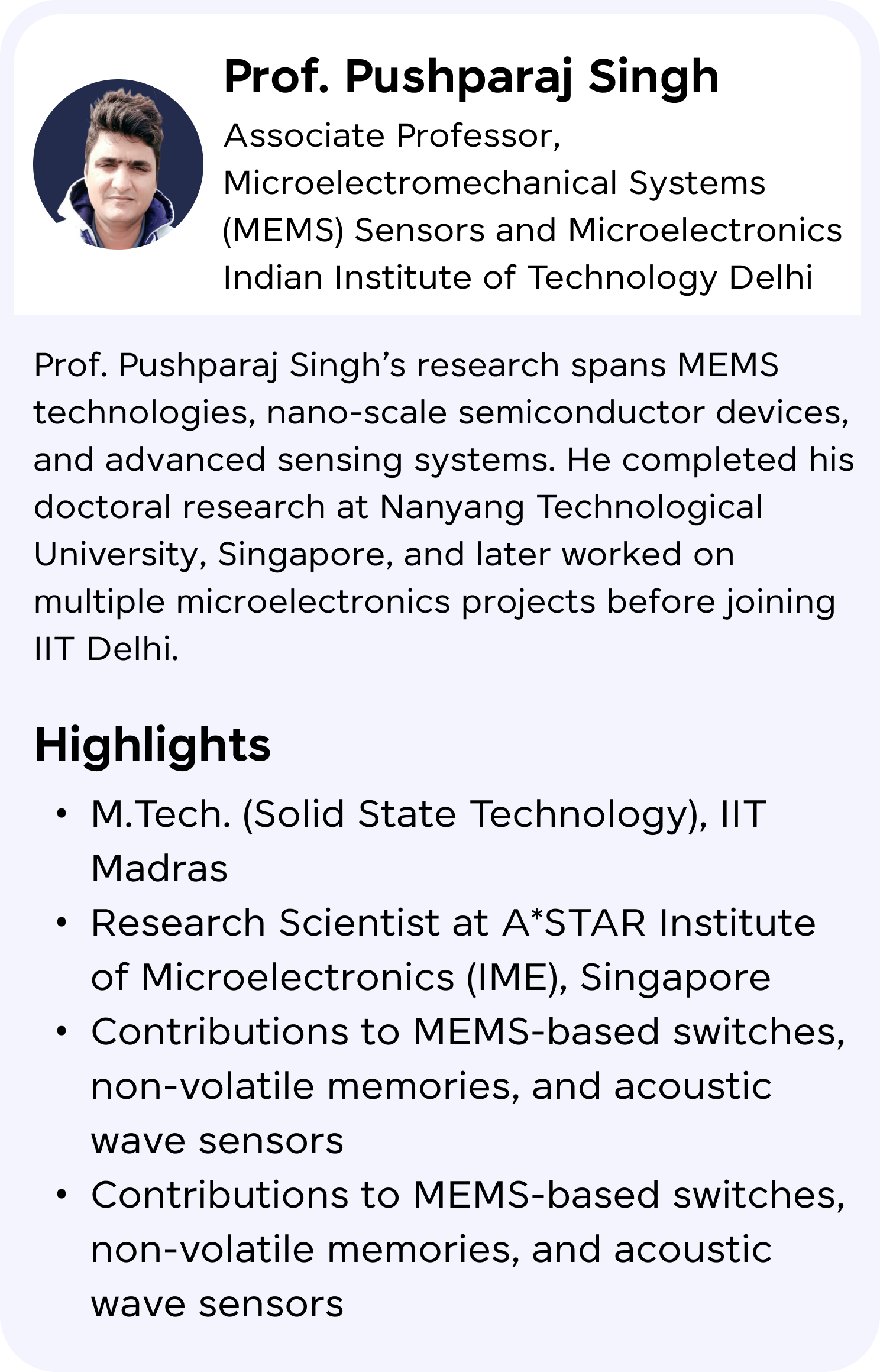
Associate Professor,
Microelectromechanical Systems (MEMS) Sensors and Microelectronics,
Indian Institute of Technology Delhi
Prof. Pushparaj Singh’s research spans MEMS technologies, nano-scale semiconductor devices, and advanced sensing systems. He completed his doctoral research at Nanyang Technological University, Singapore, and later worked on multiple microelectronics projects before joining IIT Delhi.
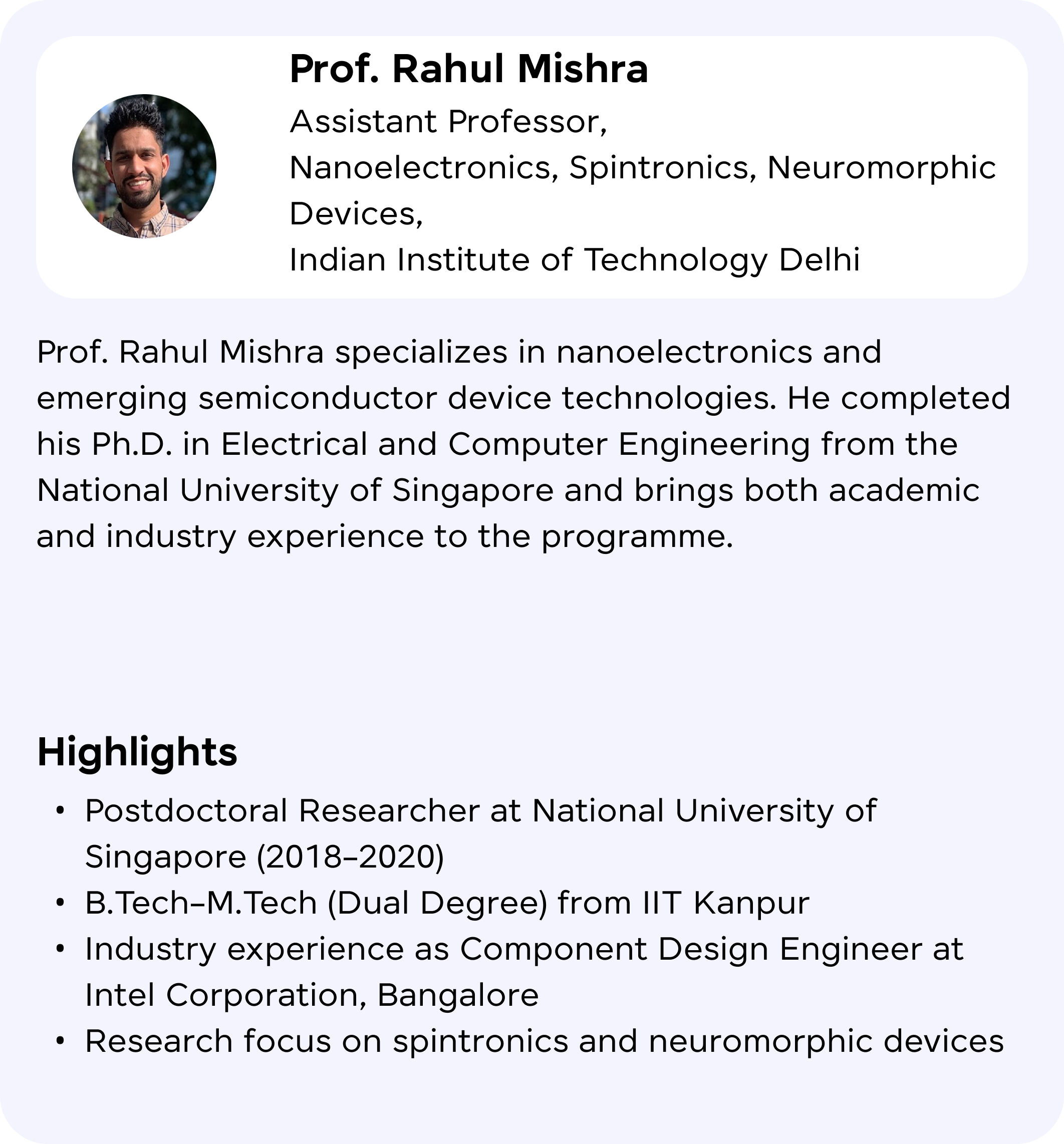
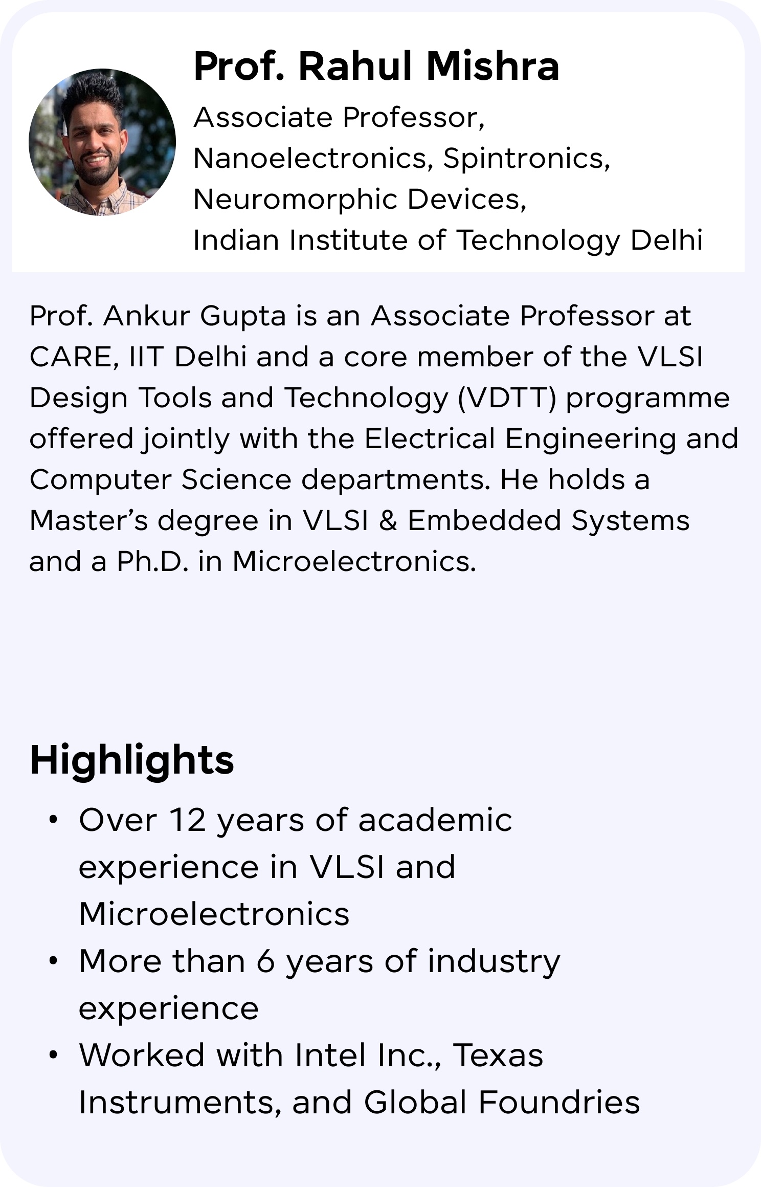
Assistant Professor,
Nanoelectronics, Spintronics, Neuromorphic Devices,
Indian Institute of Technology Delhi
Prof. Rahul Mishra specializes in nanoelectronics and emerging semiconductor device technologies. He completed his Ph.D. in Electrical and Computer Engineering from the National University of Singapore and brings both academic and industry experience to the programme.
Dr. Seema Sharma, head of the Department of Management Studies at IIT Delhi, specializes in Economics and Entrepreneurship, with research published in leading international journals.
She teaches Business Economics, Macroeconomic Environment, and Data Analysis to MBA and PhD students.
Dr. Sharma has presented globally and received awards like the ‘Outstanding Young Faculty Fellowship Award’ from IIT Delhi and the ‘Best Professor in Economics Award’ by Hindustan Unilever-BSA-Dewang Mehta Business School.
Dr. Gourav Dwivedi, an Assistant Professor in the Department of Management Studies at IIT Delhi, focuses on Operations and Supply Chain Management.
With over a decade of experience in both academia and industry, Dr. Dwivedi has contributed to various engineering service projects, particularly for Fortune 500 companies.
In academia, he has participated in collaborative research and consulting projects with national and international organizations, resulting in publications in leading journals. His research interests include Distributed Manufacturing, Supply Chain, Logistics Modelling, Industry 4.0, Behavioral Operations, Business Sustainability, and Systems Thinking.
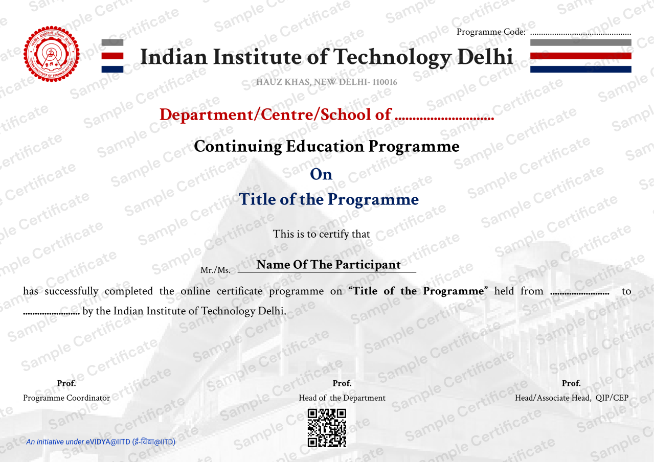
Showcase your Certificate of Completion from CEP, IIT Delhi and demonstrate validated expertise in digital VLSI design across the complete RTL to GDSII flow.
Participation Certificate
Candidates who maintain a minimum of 50% attendance will receive a Certificate of Participation from IIT Delhi's CEP.
Completion Certificate
Candidates who score at least 60% marks overall and maintain a minimum of 50% attendance will be awarded a Certificate of Completion from IIT Delhi's CEP.
*Note: Only e-certificates will be issued by Continuing Education Programme (CEP), IIT Delhi
Certificate of Completion from CEP, IIT Delhi that strengthens your credibility in the semiconductor domain
Comprehensive coverage of the RTL to GDSII digital VLSI design flow
Expert guidance from IIT Delhi faculty through live sessions over 6 months
Hands-on learning through structured projects and practical design exposure
Limited academic recognition in the semiconductor domain
Focus on isolated tools rather than the full chip design lifecycle
Lack structured progression from fundamentals to advanced implementation
Offer limited faculty interaction and research-led academic depth
₹1,35,000 + GST
Note:
Withdrawal and Refund:
Candidates can withdraw within 15 days from the programme start date. A total of 80% of the total fee received will be refunded. However, the applicable tax amount paid will not be refunded on the paid amount.
Component | Date | Amount in ₹* |
|---|---|---|
Application Fee ** | To be Paid at the time of Application | ₹1,000 |
1st Installment | Within 1 Week of offer rollout | ₹54,000 |
2nd Installment | 30th July 2026 | ₹54,000 |
3rd Installment | 10th Sep 2026 | ₹27,000 |
Note:
Application Closure Date | 24th July 2026 |
Programme Start Date | 26th July 2026 |
This voucher is offered by HCL GUVI Edtech, IIT Delhi is not responsible for this
Note:
Withdrawal and Refund:
Component | Date | Amount in ₹* |
|---|---|---|
Application Fee ** | To be Paid at the time of Application | ₹1,000 |
1st Installment | Within 1 Week of offer rollout | ₹54,000 |
2nd Installment | 30th July 2026 | ₹54,000 |
3rd Installment | 10th Sep 2026 | ₹27,000 |
Note:
Application Closure Date | 18th June, 2026 |
Programme Start Date | 26th July 2026 |
Refer Your friend to our IIT Delhi Digital VLSI Design Programme &
Get ₹10,000 Worth of Amazon Voucher
This voucher is offered by HCL GUVI Edtech, IIT Delhi is not responsible for this
Advance your semiconductor career with the CEP, IIT Delhi’s Digital VLSI Design certificate programme and build hands-on skills in RTL-to-GDSII design, verification, advanced chip implementation, and more. Perfect for beginners and working professionals alike!
Best Suited for:
Working professionals, Graduates aspiring to build a career in VLSI, and job seekers
*Travel and accommodation cost will be borne by the participants. IIT Delhi is not responsible for the same.
This structured curriculum guides you through CMOS design, RTL development, synthesis, verification, physical design, and low-power methodologies, covering the complete RTL to GDSII journey.
Eligibility Criteria
Candidates from Electronics, Electrical, Physics, Computer Science, or related backgrounds from a recognised university or institution are eligible.
Suitable for working professionals, graduates aspiring to build a career in VLSI, and job seekers.
Fresh graduates with an interest in semiconductor and VLSI technologies can also apply.
Admission Criteria
This programme builds deep technical capability across the complete digital VLSI design lifecycle, combining theory, tool-based learning, and hands-on implementation experience.
Module 1
CMOS ASIC Design Flow
MOS Device Physics
CMOS Inverter
Combinational and Sequential Logic Gates
Module 2
Introduction to Linux
Scripting VLSI
VLSI Design Flow
RTL Coding and Design Styles
Module 3
Logic Synthesis Concepts and Optimization
Static Timing Analysis and Timing Concepts
Power-Aware Synthesis
Module 4
Scan Chain Insertion, ATPG & BIST
Fault Models and Fault Coverage Metrices
Soft Errors, Reliability & Resilience in Nano-Scale VLSI
Module 5
Floor planning, Placement and Routing
CTS and Power Planning
Advanced Node Challenges: FinFET, EUV Lithography, Double Patterning
Module 6
Low Power Design Methodologies
Sources of Power Dissipation
UPF/CPF for Power-Aware Design
Module 7
Introduction to Analog IC Design
PLL & Clock Generation Circuits
Mixed Signal Design
Module 8
Scan Chain Insertion, ATPG & BIST
Fault Models and Fault Coverage Metrices
Soft Errors, Reliability & Resilience in Nano-Scale VLSI
Projects
Learners apply theoretical concepts to real-world VLSI design challenges, developing practical skills, EDA tool proficiency, and industry-ready problem-solving capability.
Step 1
Select the Certificate Programme in Digital VLSI Design and complete your registration.
Step 2
Connect with our Programme Advisors for guidance and submit the application fee to move forward.
Step 3
Get your documents verified and appear for an interview if required.
Step 4
Receive your Offer Letter from the CEP, IIT Delhi and confirm your acceptance.
Step 5
Pay the programme fees to secure your seat.
Step 6
Complete onboarding and begin your learning journey in the Digital VLSI Design Programme.
Aspiring VLSI Professionals
Individuals looking to build a strong foundation in digital VLSI design and enter the rapidly growing semiconductor industry.
Working Engineers & Technologists
Professionals seeking to upskill in chip design, synthesis, physical implementation, and low-power methodologies to transition into semiconductor-focused roles.
Electronics, Electrical & CS Graduates
Graduates and diploma holders aiming to develop industry-relevant VLSI expertise and pursue careers in RTL to GDSII design domains.
Showcase your Certificate of Completion from CEP, IIT Delhi and demonstrate validated expertise in digital VLSI design across the complete RTL to GDSII flow.
Participation Certificate
Candidates who maintain a minimum of 50% attendance will receive a Certificate of Participation from IIT Delhi's CEP.
Completion Certificate
Candidates who score at least 60% marks overall and maintain a minimum of 50% attendance will be awarded a Certificate of Completion from IIT Delhi's CEP.
*Note: Only e-certificates will be issued by Continuing Education Programme (CEP), IIT Delhi
₹1,35,000 + GST
Note:
Withdrawal and Refund:
Component | Date | Amount in ₹* |
|---|---|---|
Application Fee ** | To be Paid at the time of Application | ₹1,000 |
1st Installment | Within 1 Week of offer rollout | ₹54,000 |
2nd Installment | 30th July 2026 | ₹54,000 |
3rd Installment | 10th Sep 2026 | ₹27,000 |
Note:
* GST @ 18% will be charged extra in addition to the fees
** The application fee of ₹1,000 + 18% GST is non-refundable and non-transferable. This fee is additional and not adjusted against the total programme fee.
Application Closure Date | 24th July 2026 |
Programme Start Date | 26th July 2026 |
This voucher is offered by HCL GUVI Edtech, IIT Delhi is not responsible for this
This programme is offered by the Continuing Education Programme (CEP), IIT Delhi.
It is a 6-month live online programme with live online sessions every Sunday from 10:00 AM to 1:00 PM IST.
Graduates or diploma holders from recognised institutions are eligible to apply. Preference may be given to candidates with relevant academic background or experience.
Selection is based on application review, academic background, and verification conducted by IIT Delhi Programme Coordinator. An interview may be required.
The total programme fee is ₹1,35,000 + GST. A ₹1,000 non-refundable application fee is payable at the time of applying. The remaining fee can be paid in installments upon selection.
Yes. An 80% refund (excluding GST) is available if withdrawal is requested within 15 days of the first session.
Yes, recordings of live sessions will be available for participants throughout the programme duration.
Participants meeting the evaluation criteria will receive a Certificate of Completion from CEP, IIT Delhi. Those meeting minimum attendance requirements but not evaluation thresholds may receive a Participation Certificate. Only e-certificates are issued.
The programme covers the complete digital VLSI design flow including CMOS design, RTL development, synthesis, static timing analysis, design for testability, physical design, low-power methodologies, and advanced semiconductor technologies.
Yes, a three - day IIT Delhi campus immersion is included towards the end of the programme. Travel and accommodation cost will be borne by the participants. IIT Delhi is not responsible for the same.
By submitting, I agree to be contacted via phone, SMS, or email for offers & products, even if I am on a DNC/NDNC list.
Final Step! OTP Verification